Semiconductor device and its manufacturing method

a semiconductor device and manufacturing method technology, applied in the direction of semiconductor devices, electrical devices, transistors, etc., can solve the problems of increasing production costs and difficult to obtain a denser semiconductor device, and achieve the effect of high patterning accuracy

Inactive Publication Date: 2004-07-15
GK BRIDGE 1
View PDF0 Cites 15 Cited by
  • Summary
  • Abstract
  • Description
  • Claims
  • Application Information

AI Technical Summary

Benefits of technology

0014] The recess may be filled with the plate electrode and the capacitance dielectric. In this case, the total thickness of the conductor film of which the plate electrode is formed and the capacitance dielectric is one-half or more of the width of the recess. Therefore, the top surface of the conductor film is planarized above the recess. Thus, a memory cell transistor including a fine gate electrode with a high patterning accuracy can be obtained.
0015] The semiconductor device further comprises an upper dielectric provided on the conductor film for forming the plate electrode, wherein the total thickness of the upper dielectric, the conductor film of which the plate electrode is formed and the capacitance dielectric is one-half or more of the width of the recess. Therefore, also when an antireflection coating and a hard mask are to be provided, the flatness of a portion of the upper dielectric located above the recess can be maintained.

Problems solved by technology

However, the above-described known merged DRAM / logic devices have the following problems.
Processes for fabricating the trench-capacitor-type and stack-type merged DRAM / logic devices additionally involve complicated process steps to form a memory cell capacitor as well as a memory cell transistor.
Consequently, the yield enhancement of the devices becomes increasingly difficult in addition to prolonging the development period for design changes or the like and the period required for fabrication of the devices, leading to an increase in production cost.
Therefore, it becomes hard to obtain a denser semiconductor device while embedding a high-capacity DRAM in a logic circuit.

Method used


Image

  • Semiconductor device and its manufacturing method
  • Semiconductor device and its manufacturing method
  • Semiconductor device and its manufacturing method

Examples


first embodiment

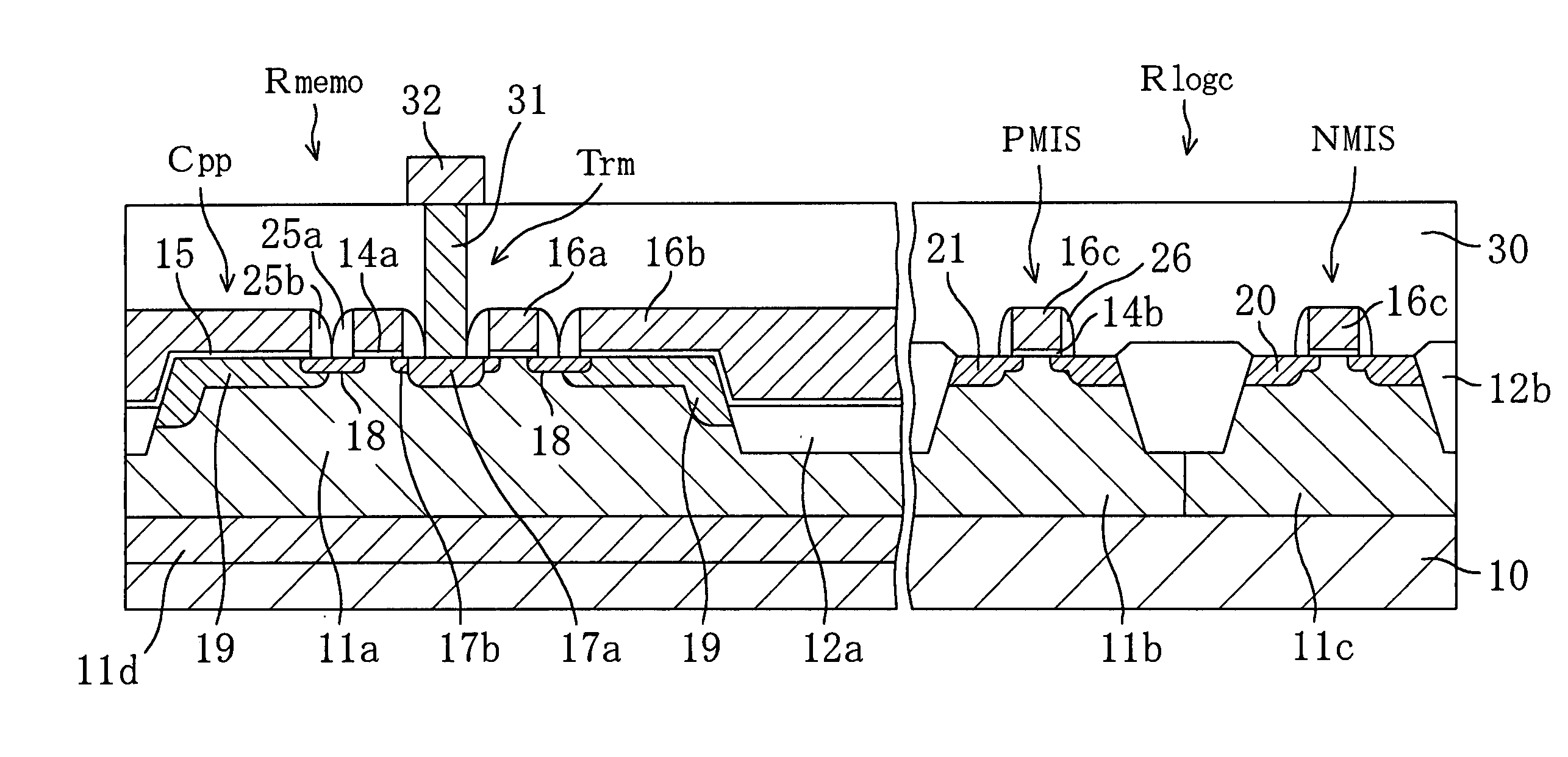
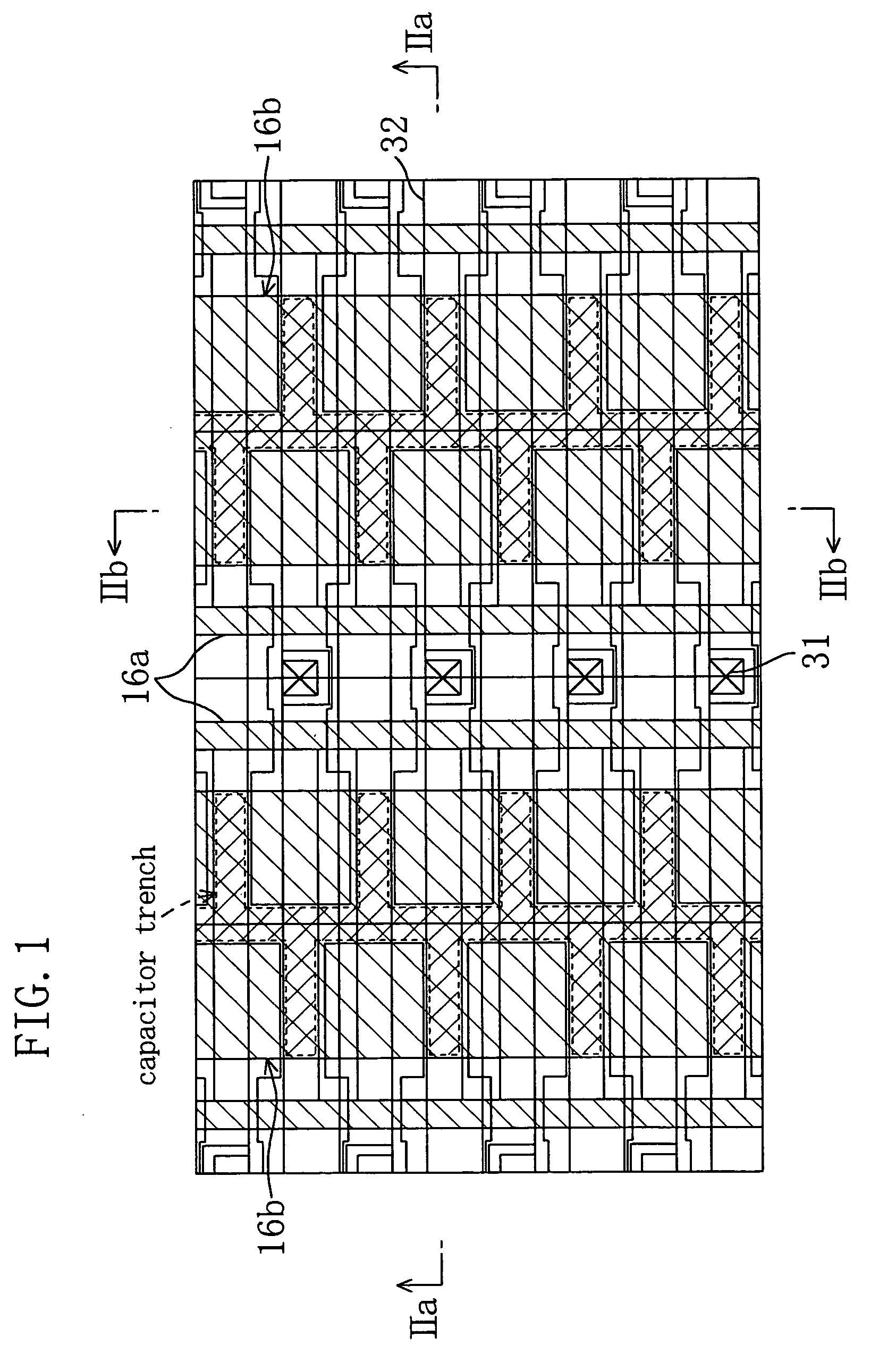
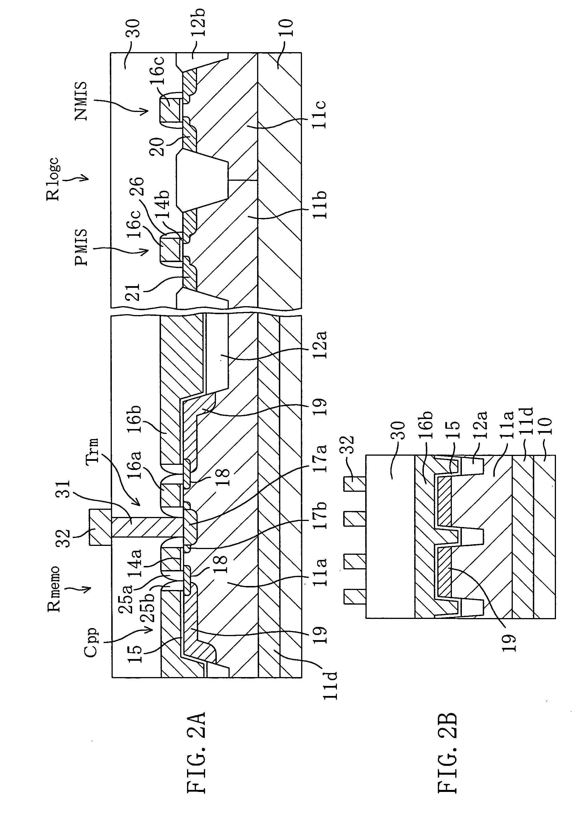
[0042] FIG. 1 is a plan view illustrating the structure of a memory of a semiconductor device according to the present invention. FIGS. 2A and 2B are cross sectional views taken along the lines IIa-IIa and IIb-IIb shown in FIG. 1, respectively. Although FIG. 2A illustrates cross sectional structures of a memory region Rmemo and a logic circuit region Rlogc of the semiconductor device, FIGS. 1 and 2B do not illustrate the cross sectional structure of the logic circuit region Rlogc.

[0043] As shown in FIGS. 1, 2A and 2B, the semiconductor device of this embodiment includes a p-type silicon substrate 10, a p-well 11a provided in the memory region Rmemo of the silicon substrate 10, an n-well 11b and a p-well 11c both provided in the logic circuit region Rlogc of the silicon substrate 10, and a deep n-well 11d surrounding the bottom part of the p-well 11a located in the memory region Rmemo, i.e., the device has a so-called triple-well structure. The device comprises a shallow trench isola...

second embodiment

[0079] FIG. 6 is a plan view illustrating the structure of a memory of a semiconductor device according to a second embodiment of the present invention. FIGS. 7A and 7B are cross sectional views taken along the lines VIIa-VIIa and VIIb-VIIb shown in FIG. 6, respectively. FIG. 7A illustrates cross sectional structures of the memory region Rmemo and the logic circuit region Rlogc of the semiconductor device. However, the cross sectional structure of the logic circuit region Rlogc is not shown in FIGS. 6 and 7B.

[0080] As shown in FIGS. 6, 7A and 7B, the semiconductor device of this embodiment includes a p-type silicon substrate 10, a p-well 11a provided in the memory region Rmemo of the silicon substrate 10, an n-well 11b and a p-well 11c both provided in the logic circuit region Rlogc of the silicon substrate 10, and a deep n-well 11d surrounding the bottom region of the p-well 11a located in the memory region Rmemo, i.e., the device has a so-called triple well structure. The device c...

third embodiment

[0111] The planar capacitor according to the first embodiment can be arranged so as to fill in the upper parts of the capacitor trench and the trench of the shallow trench isolation that are described in the second embodiment.

[0112] FIG. 10 is a plan view illustrating the structure of a memory of a semiconductor device according to a third embodiment of the present invention. FIGS. 11A and 11B are cross sectional views taken along the lines XIa-XIa and XIb-XIb shown in FIG. 10, respectively. Although FIG. 11A illustrates cross sectional structures of a memory region Rmemo and a logic circuit region Rlogc of the semiconductor device, FIGS. 10 and 11B do not illustrate the cross sectional structure of the logic circuit region Rlogc.

[0113] As shown in FIGS. 10, 11A and 11B, the semiconductor device of this embodiment includes a p-type silicon substrate 10, a p-well 11a provided in the memory region Rmemo of the silicon substrate 10, an n-well 11b and a p-well 11c both provided in the l...


PUM


Abstract

A memory cell transistor and a planar capacitor are provided in a memory region, and both transistors of a CMOS device are provided in a logic circuit region. A capacitance dielectric 15 and a plate electrode 16b of the planar capacitor are provided over a trench shared with a shallow trench isolation 12a, and the upper part of the trench is filled with the capacitance dielectric 15 and the plate electrode 16b. An n-type diffusion layer 19 that is a storage node is formed, with an end region thereof extending along one side of the upper part of the trench, to a region of the substrate overlapping with the shallow trench isolation 12a. The area of a part of the substrate functioning as a capacitor can be increased without increasing the substrate area.

Description

[0001] The present invention relates to a semiconductor storage device and a method for fabricating the same, and more particularly to those that are applied to a so-called DRAM-embedded logic LSI in which a DRAM is embedded in a logic chip.[0002] In recent years, DRAM-embedded devices in which a high-performance logic circuit and a DRAM memory are combined together have been made practical for multimedia devices requiring miniaturization, a high memory capacity and a high data transfer rate. The DRAM-embedded devices are broadly classified into a trench capacitor type in which a capacitor as an information storage unit of a DRAM memory cell is provided in a trench of a semiconductor substrate and a stack capacitor type in which a capacitor and an electrode are three-dimensionally stacked above a principal surface of a semiconductor substrate.[0003] On the other hand, attention is again focused on a device in which a so-called planar (MOS structure) DRAM and a logic circuit are merg...

Claims


Application Information

Patent Timeline
Patent Type & Authority Applications(United States)
IPC IPC(8): H01L21/335H01L21/8242H01L27/02H01L27/10H01L27/105H01L27/108
CPCH01L27/0207H01L27/105H01L27/10897H01L27/10894H01L27/10852H10B12/50H10B12/09H10B12/033H10B12/00
Inventor OGAWA, HISASHINAKAOKA, HIROAKIKAJIYA, ATSUHIROHASHIMOTO, SHINEGASHIRA, KYOKO
Owner GK BRIDGE 1
Why Eureka
Try Eureka