

Planar light source and display device using the same
a technology of display device and light source, which is applied in the direction of instruments, polarising elements, non-linear optics, etc., can solve the problems of affecting the efficiency of light emission, the complexity of the light-emitting layer itself, and the inability to raise the percent utilization of light to greater than 50%, so as to achieve the effect of remarkably reducing the invention and relatively great difference in refractive index between the two materials
- Summary
- Abstract
- Description
- Claims
- Application Information
AI Technical Summary
Benefits of technology
Problems solved by technology
Method used
Image

Examples
example 1
[0126] (1) Preparation of Organic EL Element
[0127] A glass substrate was subjected to DC sputtering on one side thereof using an ITO ceramic target (In2O3:SnO2=90% by weight:10% by weight) to form a transparent electrode (anode) made of ITO layer to a thickness of 100 nm. Thereafter, the ITO layer was etched with a photoresist to form a pattern having a luminous area of 15 mm.times.15 mm. Subsequently, the ITO layer was subjected to ultrasonic cleaning and then to ozone cleaning using a low voltage UV lamp. Subsequently, thin organic layers were sequentially vacuum-deposited on the ITO layer under the following conditions.
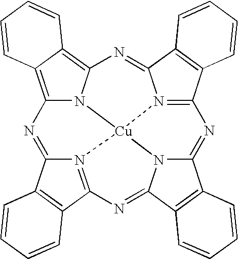
[0128] In some detail, CuPc (chemical formula 1) was vacuum-deposited on the ITO layer as a hole-injecting layer at a rate of 0.3 nm / s to a thickness of 15 nm.
[0129] [Chemical Formula 1] 2
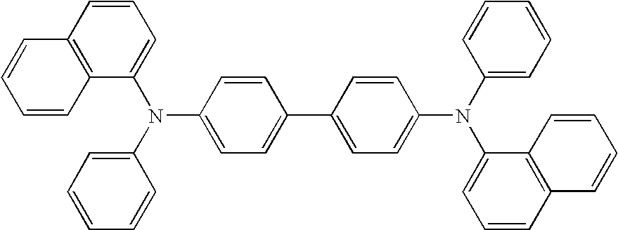
[0130] .alpha.-NPD (chemical formula 2) was then vacuum-deposited on the CuPc layer as a hole-transporting layer at a rate of 0.3 nm to a thickness of 50 nm.
[0131] [Chemical Formu...
example 2
[0151] An anisotropic scattering film was prepared in the same manner as in the step (2) of preparing an anisotropic scattering color conversion layer of Example 1 except that 3-(2-benzothiazolyl)-7-diethylaminocoumari-ne (coumarine 6) represented by the chemical formula (5) was not added. Subsequently, the transparent color conversion film free from light scattering prepared in Comparative Example 2 was stuck to the glass substrate of an organic EL element prepared in the same manner as in Example 1 with an acrylic transparent adhesive layer interposed therebetween. The aforementioned anisotropic scattering film was then stuck to the aforementioned color conversion film with an acrylic transparent adhesive layer interposed therebetween.
[0152] Under these conditions, a voltage of 10 V was then applied to the organic EL element. As a result, current passed through the organic EL element on substantially the same order as mentioned in Example 1 to cause the emission of green electrolu...
PUM
 Abstract
Description
Claims
Application Information