Integrated circuit, semiconductor device comprising the same, electronic device having the same, and driving method of the same

a technology of integrated circuits and semiconductor devices, applied in the direction of identification means, digital storage, instruments, etc., can solve the problems of difficult to obtain a material with a drastically low dielectric constant, difficult to produce a compact flat panel display, and optimization of materials of dielectric films

Inactive Publication Date: 2004-12-09
SEMICON ENERGY LAB CO LTD
View PDF36 Cites 40 Cited by
  • Summary
  • Abstract
  • Description
  • Claims
  • Application Information

AI Technical Summary

Problems solved by technology

Generally, a flat panel display formed by using an inexpensive glass substrate has a problem in that, the periphery of a pixel portion (frame area) which is used for mounting occupies larger area of the substrate as resolution becomes high, and this makes it difficult to produce a compact flat panel display.
Therefore, it is considered that there is a limitation with regard to a method for mounting an IC which is formed by using a single crystal silicon wafer on a substrate, and thus technology for monolithically forming an integrated circuit and a pixel portion onto a glass substrate, namely development of a system-on-panel is expected to be advanced.
However, there is a limitation for the optimization of a material of a dielectric film, and it is thus difficult to obtain a material having a drastically low dielectric constant.
In addition, a DRAM formed with a three-dimensionalized capacitor, such as a stack memory cell and a trench memory cell, is effective for reduction in tip size, however, it is disadvantageous in that cost per bit becomes high as its manufacturing steps are complicated as compared to those of DRAM using a planar memory cell.
Therefore, it is difficult to achieve high integration of DRAM by utilizing its advantages of large memory capacity and low cost.
However, when overwriting new data onto previous data, it is required before writing the new data that the previous data is completely deleted by raising a potential of the first gate electrode to discharge (purge) the accumulated charges.
Also, when a thin film transistor is compared to a transistor formed by using a single crystal semiconductor film, it is generally thought that charges are easily leaked out due to a grain boundary in an active layer, leading to a short holding time of charges.
In particular, in the case of multi-state data having three states or more, the difference of the charge amount between each state tends to become smaller as the number of states increases as four, five, and more, thus it is difficult to keep accuracy of data.
However, as for a transistor formed by using a single crystal semiconductor film, the conventional process has to be made a drastic change in forming two gate electrodes interposing an active layer, thereby leading to more complicated steps and further to a high cost.
In other words, the film has a structure in which crystal lattices are continuously joined at the crystal grain boundary, and which is very hard to create trap levels ascribable to crystal defects and the like.
A single crystal SOI substrate has a problem in that it cannot easily provide a very thin single crystal silicon film, whereas a thin film transistor can provide a very thin active layer by depositing a semiconductor layer.
However, a semiconductor film crystallized by these methods is inferior in matching of the two different crystal grains at a crystal grain boundary as compared to the case of using a metal catalyst, thus it tends to create a number of trap levels ascribable to crystal defects and the like.
When there are a number of such trap levels, electron hole pairs are generated due to the level that serves as a nucleus, therefore, charge retention characteristics are deteriorated.
However, the thin film transistor used for switching may not necessarily be of a dual gate type, and a single gate thin film transistor that is present only in either side of an active layer may also be employed.

Method used


Image

  • Integrated circuit, semiconductor device comprising the same, electronic device having the same, and driving method of the same
  • Integrated circuit, semiconductor device comprising the same, electronic device having the same, and driving method of the same
  • Integrated circuit, semiconductor device comprising the same, electronic device having the same, and driving method of the same

Examples


embodiment 1

[0154] A DRAM comprising a switching element as well as a TFT which is used as a memory element is described.

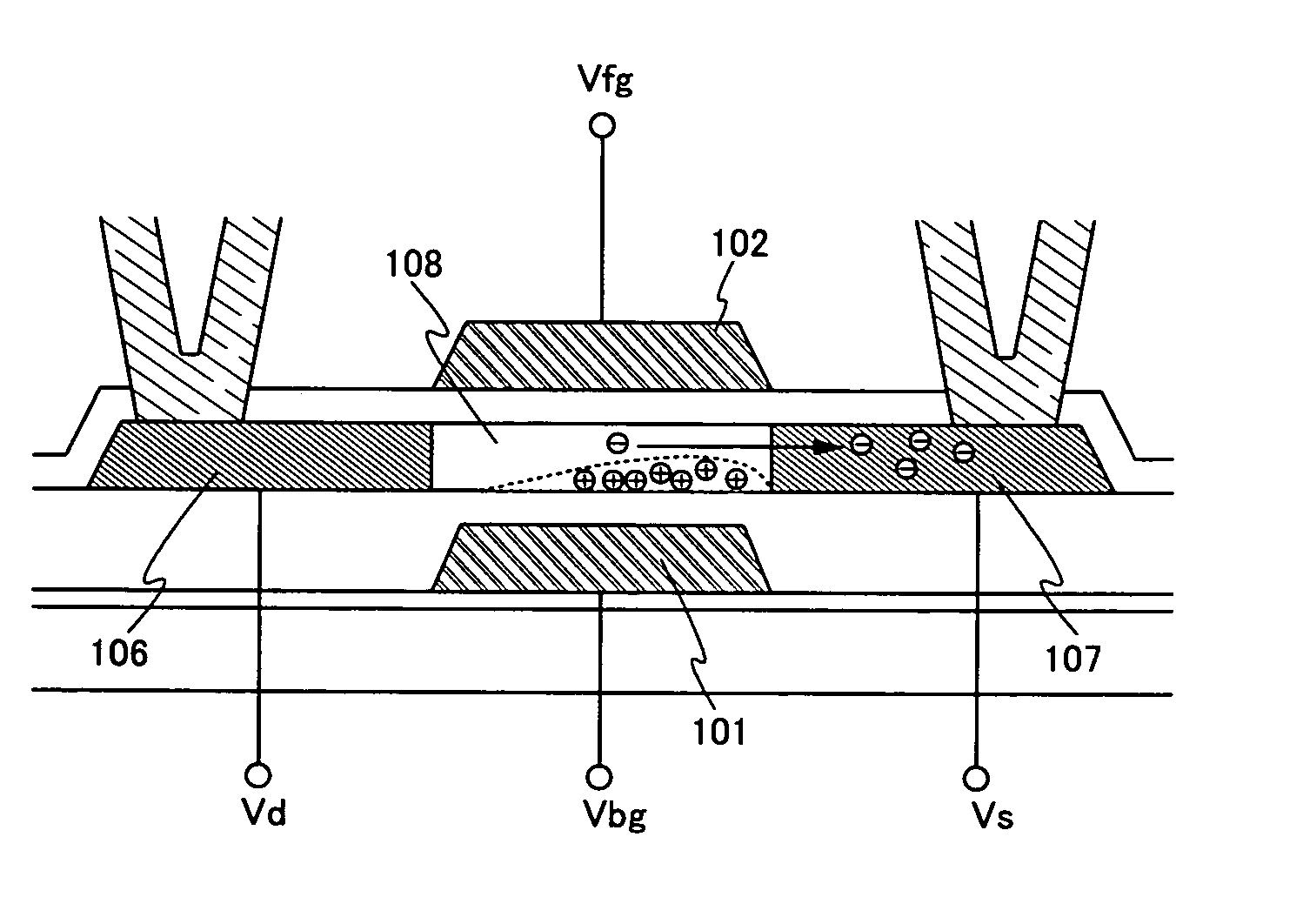
[0155] An example of a circuit diagram of a cell array of a DRAM according to the present embodiment is shown in FIG. 8A. The cell array shown in FIG. 8A comprises four memory cells (Cell1, Cell2, Cell3, and Cell4), and each memory cell is provided with a TFT 800 which functions as a memory element and a TFT 801 which functions as a switching element. Although four memory cells are disposed in the memory cell array in FIG. 8A, the number of memory cells is, needless to mention, not limited to this.

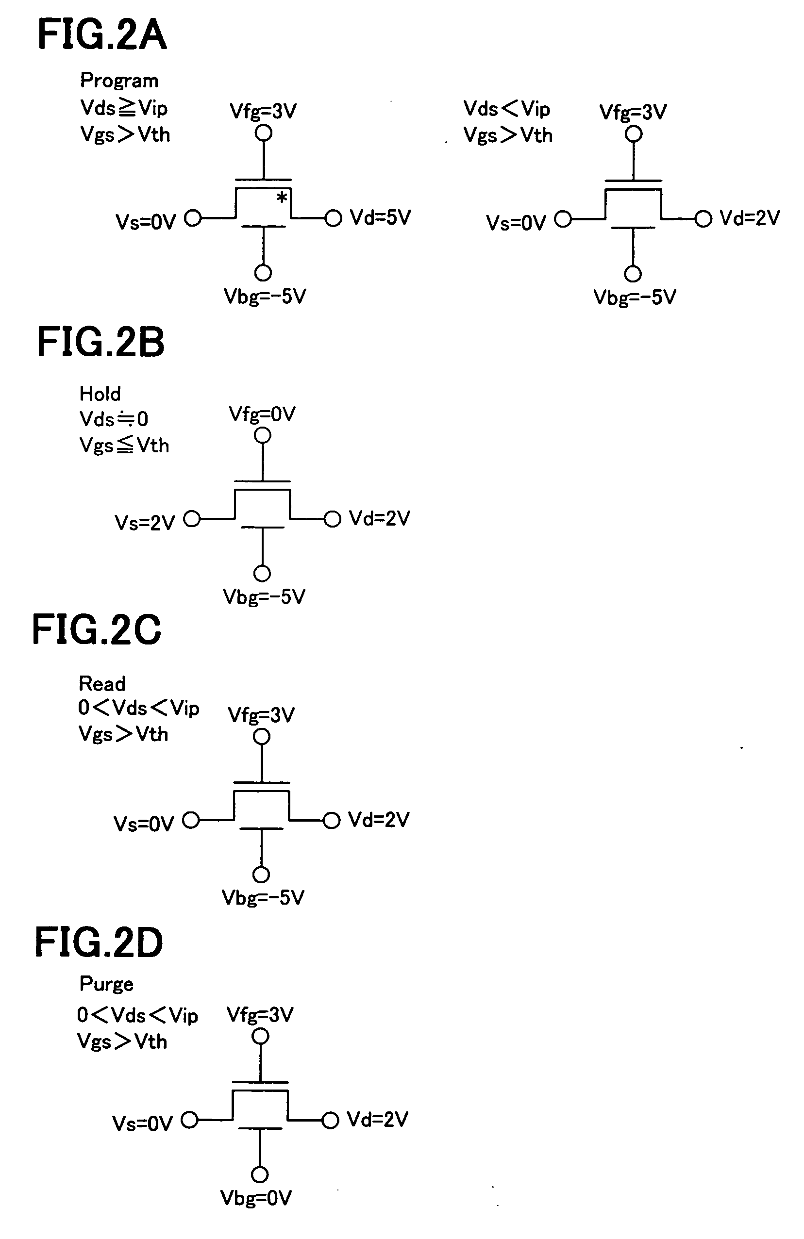
[0156] The TFT 800 in each memory cell receives potentials Vbg and Vfg from word lines WLb and WLf respectively, and a potential Vs from a source line SL. The supply of a potential Vd from a bit line BL is controlled by the TFT 801. Switching of the TFT 801 is controlled by a potential supplied to its gate electrode from a select line SeL. Note that, the layout of each wiring is not...

embodiment 2

[0164] Described in this embodiment is a structure of a memory cell of a DRAM which is mounted on the integrated circuit of the invention.

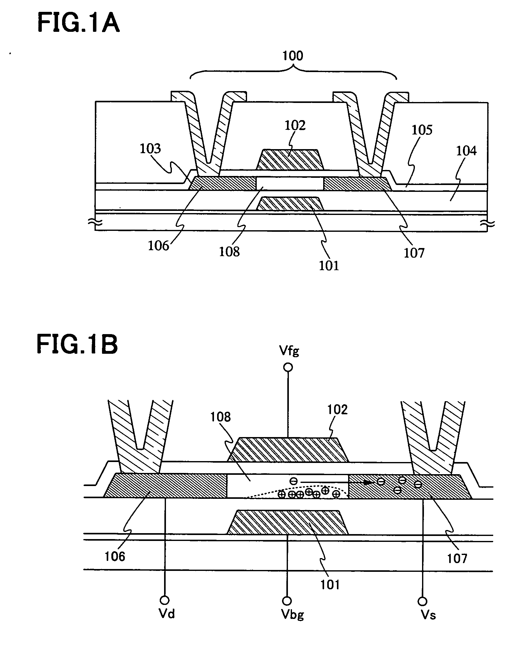
[0165] FIG. 9A shows a top plan view of memory cell of the present embodiment. A memory cell shown in FIG. 9A comprises a TFT 901 which functions as a memory element. Reference numeral 902 denotes a bit line BL, 903 denotes a source line SL, and 904 denotes a word line WLf. As shown in FIG. 9A, the source line SL 903 is obtained by patterning the same conductive layer as a word line WLb 906.

[0166] FIG. 9B shows a top plan view of the memory cell shown in FIG. 9A, prior to the formation of the bit line BL 902 on a top layer. Reference numeral 905 denotes an active layer of the TFT 902. The word line WLf 904 partially overlaps with the active layer 905 with a second insulating layer (not shown) interposed therebetween, and it functions as a second electrode. In this embodiment, the word line WLf 904 is disposed between the active layer 905 and the b...

embodiment 3

[0170] In this embodiment, a configuration of a microprocessor which is one of the integrated circuits of the invention is described.

[0171] FIG. 10 shows a perspective view of a microprocessor of the present embodiment. The microprocessor comprises a substrate 400 which is mounted with a CPU 401, a main memory 403, a clock controller 404, a cache controller 405, a serial interface 406, an I / O port 407, a terminal 408, an interface 409, a cache memory 410, and the like. It is needless to mention that the schematic view of the microprocessor shown in FIG. 10 is only an example and therefore microprocessors in practice take various configurations according to their practical use.

[0172] In order to operate the CPU 401 at a higher rate, a memory which is operable at a corresponding rate to that of the CPU is required. However, when using a high capacity memory which is operable at a high rate and having an access time corresponding to an operating rate of the CPU 401, cost increases gene...


PUM


Abstract

An integrated circuit mounting a DRAM which can realize high integration without complicated manufacturing steps. The integrated circuit according to the invention comprises a DRAM in which a plurality of memory cells each having a thin film transistor are disposed. The thin film transistor comprises an active layer including a channel forming region, and first and second electrodes overlapping with each other with the channel forming region interposed therebetween. By controlling a drain voltage of the thin film transistor according to data, it is determined whether to accumulate holes in the channel forming region or not, and data is read out by confirming whether or not holes are accumulated,.

Description

[0001] 1. Field of the Invention[0002] The present invention relates to an integrated circuit mounting DRAM formed by using a thin film semiconductor film, and more particularly to a semiconductor display device (semiconductor device) comprising the integrated circuit and a driving method of the integrated circuit.[0003] 2. Description of the Related Art[0004] Generally, a flat panel display formed by using an inexpensive glass substrate has a problem in that, the periphery of a pixel portion (frame area) which is used for mounting occupies larger area of the substrate as resolution becomes high, and this makes it difficult to produce a compact flat panel display. Therefore, it is considered that there is a limitation with regard to a method for mounting an IC which is formed by using a single crystal silicon wafer on a substrate, and thus technology for monolithically forming an integrated circuit and a pixel portion onto a glass substrate, namely development of a system-on-panel i...

Claims


Application Information

Patent Timeline
Patent Type & Authority Applications(United States)
IPC IPC(8): G09F9/30G11C11/404H01L21/8242H01L27/10H01L27/108H01L27/12H01L29/78H01L29/786
CPCG11C11/404H01L27/108H01L27/12H01L29/7841H01L29/78621H01L29/78648H10B12/00
Inventor KATO, KIYOSHI
Owner SEMICON ENERGY LAB CO LTD
Why Eureka
Try Eureka