Silver alloy material, circuit substrate, electronic device, and method for manufacturing circuit substrate

a technology of silver alloy and circuit substrate, which is applied in the direction of non-linear optics, identification means, instruments, etc., can solve the problems of large equipment cost, limited usable range of silver, and significant lack of heat resistance of silver, so as to achieve high plasma resistance, high heat resistance, and strong adhesion

Inactive Publication Date: 2005-01-27
SHARP KK
View PDF8 Cites 38 Cited by
  • Summary
  • Abstract
  • Description
  • Claims
  • Application Information

AI Technical Summary

Benefits of technology

[0023] The present invention has an objective to provide a silver alloy material that can realize a material having heat resistance and strong adhesion to a glass substrate as well as high plasma resistance and good light reflectance. The present invention also has an ob

Problems solved by technology

Accordingly, a huge cost of equipment is required in the manufacturing of TFT array substrates in response to recent demands for TFT array substrates having larger size.
However, the usable range of silver is limited because of the properties of silver.
Silver significantly lacks heat resistance.
If silver is formed into a film on a glass substrate using an evaporation method, a sputtering method, or other methods, for example, the silver film generates grain growth and clouded surface when baked at about 250° C. Further, silver has weak adhesion to the glass substrate.
Therefore silver cannot be directly used as a material for forming the lines on TFT array substrates.
Further, conventional silver has low heat resistance, and the reflectance of the silver is remarkably lowered after the silver is baked at 200° C., for example.
Hence, conventional silver cannot be used if heat resistance is required during the manufacturing process.
For example, it has been difficult to use silver as a material for a light reflecting film provided on a TFT array substrate in a reflection type liquid crystal display device, for example.
However, it is difficult for one type of material

Method used


Image

  • Silver alloy material, circuit substrate, electronic device, and method for manufacturing circuit substrate
  • Silver alloy material, circuit substrate, electronic device, and method for manufacturing circuit substrate
  • Silver alloy material, circuit substrate, electronic device, and method for manufacturing circuit substrate

Examples


first embodiment

[0098] [First Embodiment]

[0099] The following will explain an embodiment of the present invention.

[0100] In the present embodiment, a silver alloy material of the present invention will be explained first, and then a TFT array substrate and liquid crystal display device using the silver alloy material will be explained.

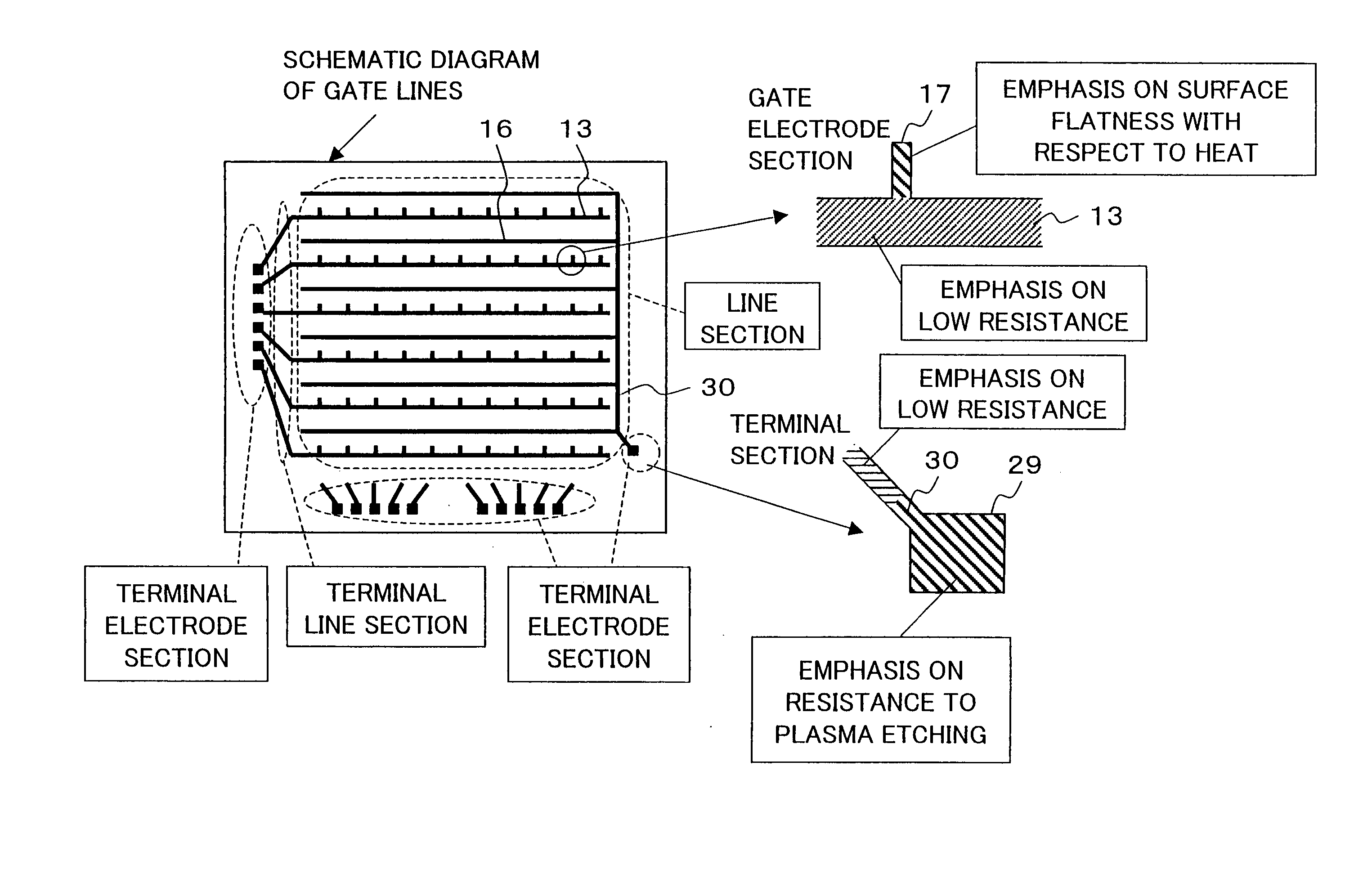
[0101] A silver alloy material of the present invention which composes lines and / or electrodes formed on an insulation substrate such as a glass substrate is arranged so as to contain silver as a main component and at least one element selected from the group consisting of tin, zinc, lead, bismuth, indium, and gallium.

[0102] With the silver alloy material as arranged above, it is possible to form lines and / or electrodes having low electric resistance, as well as high process resistance such as heat resistance, adhesion to the glass substrate, and plasma resistance.

[0103] With reference to Examples 1 through 9 and Comparative Examples 1 and 2, the following will de...

second embodiment

[0266] [Second Embodiment]

[0267] The following will explain another embodiment of the present invention with reference to FIGS. 6, 19(a), and 19(b).

[0268] In First Embodiment, the pattern formation equipment employing an ink-jet method, for example, is used in the gate line formation step 102 and the source and drain lines formation step 106.

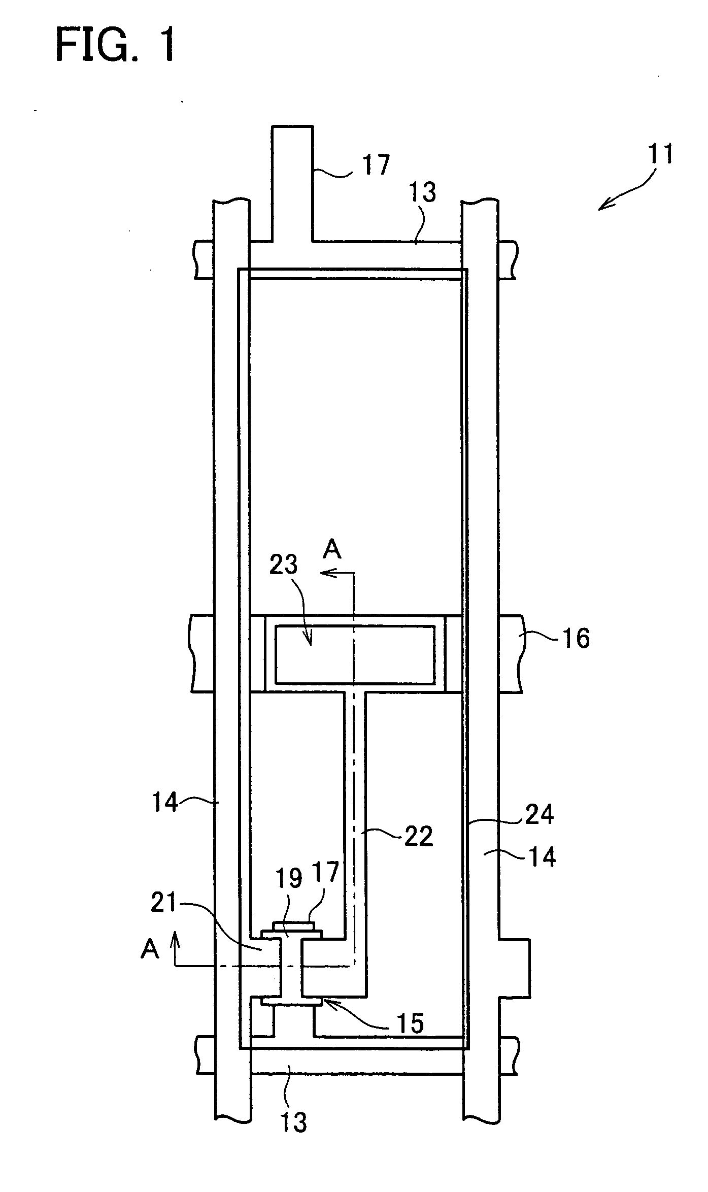
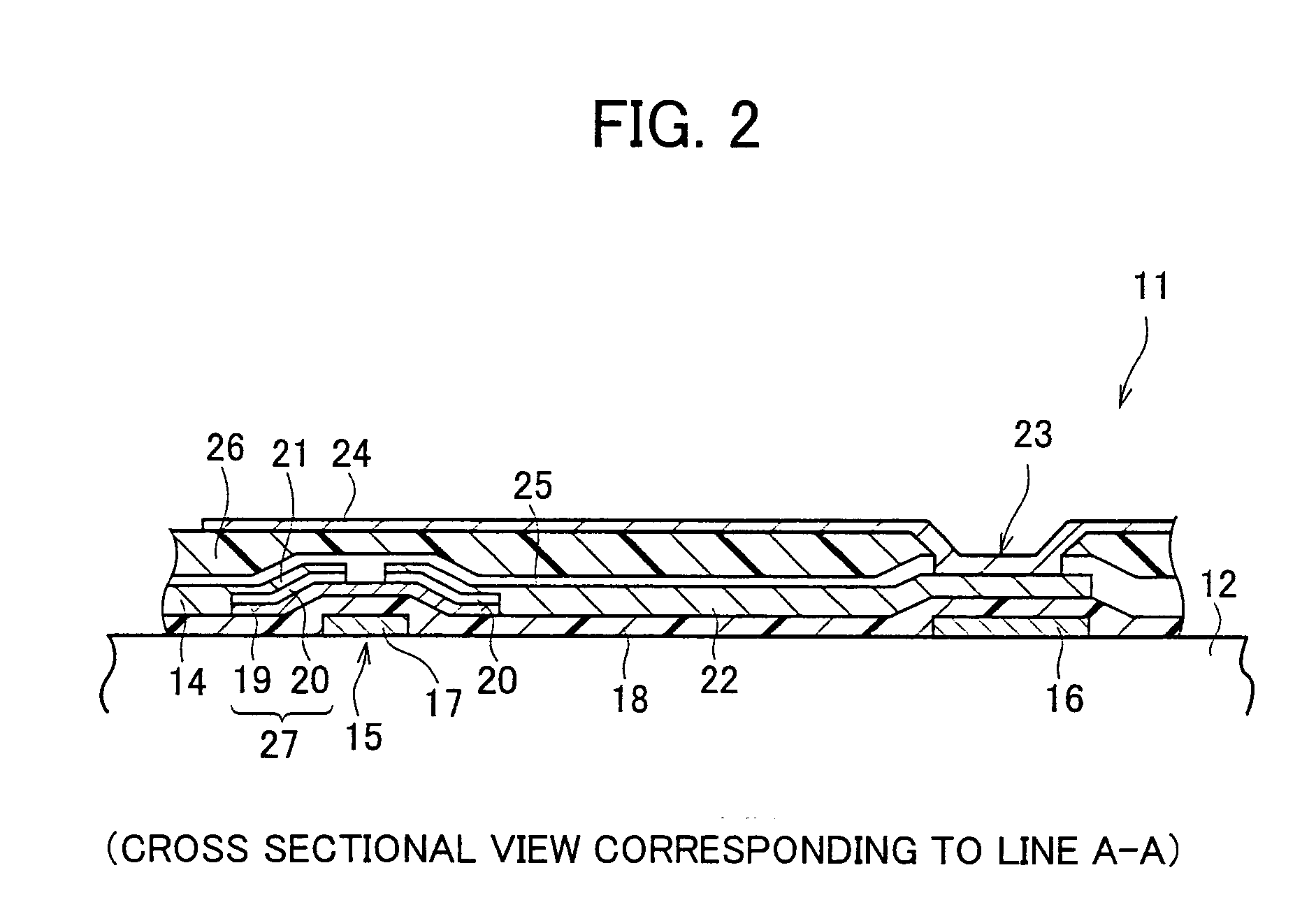
[0269] A TFT array substrate 71 in accordance with the present embodiment is produced in a manner as shown in the process flow chart of FIG. 6 as in First Embodiment, except that in the gate line formation step 102, two or more types of fluid wiring materials are used to form the lines and the like having different compositions within the substrate (separate application).

[0270] Note that, constituent elements substantially having the same function as those used in First Embodiment are given the same reference symbols, thus their explanation will be omitted here.

[0271] FIGS. 19(a) and 19(b) show a TFT array substrate 71 in accordance with the...

third embodiment

[0285] [Third Embodiment]

[0286] The following will explain a further embodiment of the present invention.

[0287] In Second Embodiment, the pattern formation equipment typified by ink-jet pattern formation equipment is used in the gate line formation step 102 to separately apply wiring materials having different compositions onto the TFT array substrate 71.

[0288] Note that, constituent elements substantially having the same function as those used in First and Second Embodiments are given the same reference symbols, thus their explanation will be omitted here.

[0289] In the present embodiment, the separate application of the wiring materials having different compositions is performed in the source and drain lines formation step 106, instead of the gate line formation step 102. Here, the wiring materials are arranged such that an amount of indium with respect to silver is 3% by weight in the source electrode 21 and source line 14, and 10% by weight in the drain electrode line 22, for ...


PUM

PropertyMeasurementUnit
Percent by massaaaaaaaaaa

Abstract

A circuit substrate of the present invention uses as component materials for gate lines and gate electrodes, silver alloy material containing silver as a main component, and at least one element selected from the group consisting of tin, zinc, lead, bismuth, indium, and gallium. It is especially preferable that the silver alloy material mainly consisting of silver and containing indium is used for the gate lines and the gate electrodes. With this, it is possible to provide silver alloy material whose resistance value, adhesion, plasma resistance, and reflection characteristics can be appropriately adjusted by the adjustment of the content of indium. Further, it is also possible to apply the alloy in accordance with the characteristic required for each part of the circuit substrate.

Description

[0001] This Nonprovisional application claims priority under 35 U.S.C. § 119(a) on Patent Application No. 200806 / 2003 filed in Japan on Jul. 23, 2003, Patent Application No. 200815 / 2003 filed in Japan on Jul. 23, 2003, Patent Application No. 185228 / 2004 filed in Japan on Jun. 23, 2004, and Patent Application No. 185264 / 2004 filed in Japan on Jun. 23, 2004, the entire contents of which are hereby incorporated by reference. FIELD OF THE INVENTION [0002] The present invention relates to a silver alloy material. The present invention relates in particular to a silver alloy material which composes lines and / or electrodes on a circuit substrate that uses an insulation substrate; a circuit substrate whose lines and / or electrodes are formed using either the above-mentioned material or fluid material such as silver alloy fluid; a method for manufacturing the circuit substrate; and an electronic device using the circuit substrate, such as a display device, a liquid crystal display device, and...

Claims


Application Information

Patent Timeline
IPC IPC(8): H01B1/02C22C5/10C23C14/14C23C14/34G02F1/1343G09F9/30H01L23/48H05K1/09
CPCC22C5/06G02F2001/136295H01B1/02H05K1/097H05K3/125H05K2201/0391H01L2924/0002H05K2203/013H01L27/124H01L27/1292H01L2924/00G02F1/136295
Inventor SAITOH, YUHICHIFUJII, AKIYOSHI
Owner SHARP KK
Why Eureka
Try Eureka