Semiconductor device and method for manufacturing the same

a semiconductor device and integrated circuit technology, applied in semiconductor devices, electrical devices, instruments, etc., can solve the problems of epitaxial crystallization in solid phase, which cannot solve the problem of epitaxial crystallization under 600° c. of temperature, and the concept of epitaxial crystallization cannot be used. , to achieve the effect of low leakage current, good crystallinity and high mobility

Inactive Publication Date: 2005-01-27
SEMICON ENERGY LAB CO LTD
View PDF99 Cites 52 Cited by
  • Summary
  • Abstract
  • Description
  • Claims
  • Application Information

AI Technical Summary

Benefits of technology

[0042] In this case, a thickness of the silicide layer obtained is determined by the temperature and time of the heat treatment (pre-annealing) and the thickness of the metal layer has almost nothing to do with it. Due to that, the very small amount of metal element introduced in the amorphous silicon film can be controlled.
[0043] The present invention also utilizes that there is a difference in degrees of crystallization when the surface of semiconductor is covered by a coating film (cover film) of silicon oxide or silicon nitride and when not covered when crystallizing a crystalline silicon TFT in a temperature at 450 to 1000° C. or preferably at 500 to 800° C. in an atmosphere containing oxygen, hydrogen or nitrogen. Such atmosphere can be an atmosphere containing oxygen, atmosphere containing hydrogen, atmosphere containing nitrogen, atmosphere containing oxygen and hydrogen, atmosphere containing oxygen and nitrogen, atmosphere containing hydrogen and nitrogen or atmosphere containing oxygen, hydrogen and nitrogen. The aforementioned crystallization can be carried out by (1) heating for A hours in the atmosphere containing oxygen and then heating for B hours in the atmosphere containing hydrogen: (2) heating for C hours in the atmosphere containing oxygen and then heating for D hours in the atmosphere containing nitrogen: (3) heating for E hours in the atmosphere containing hydrogen and then heating for F hours in the atmosphere containing oxygen: (4) heating for G hours in the atmosphere containing hydrogen and then heating for H hours in the atmosphere containing nitrogen: (5) heating for I hours in the atmosphere containing nitrogen and then heating for J hours in the atmosphere containing oxygen: (6) heating for K hours in the atmosphere containing nitrogen and then heating for L hours in the atmosphere containing hydrogen: (7) heating for M hours in the atmosphere containing oxygen, heating for N hours in the atmos...

Problems solved by technology

However, crystal barely grew under 600° C. of temperature by such method.
However, energy for parting the initial molecular chains and for keeping them in the state not to couple with other...

Method used


Image

  • Semiconductor device and method for manufacturing the same
  • Semiconductor device and method for manufacturing the same
  • Semiconductor device and method for manufacturing the same

Examples


first embodiment

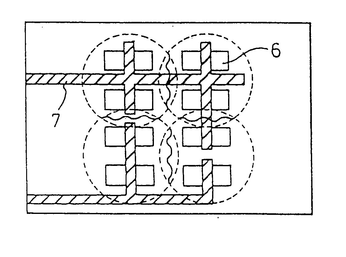
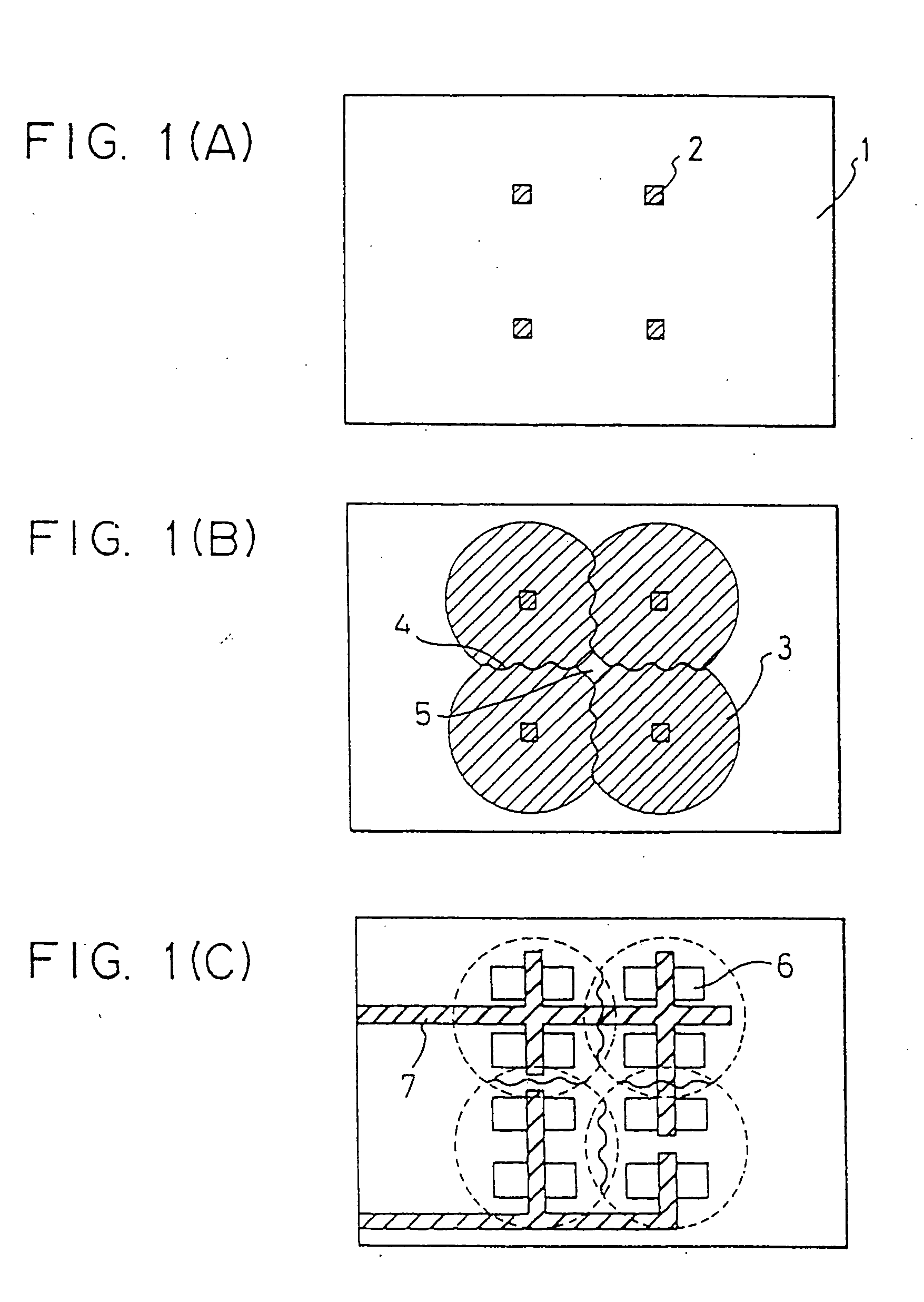
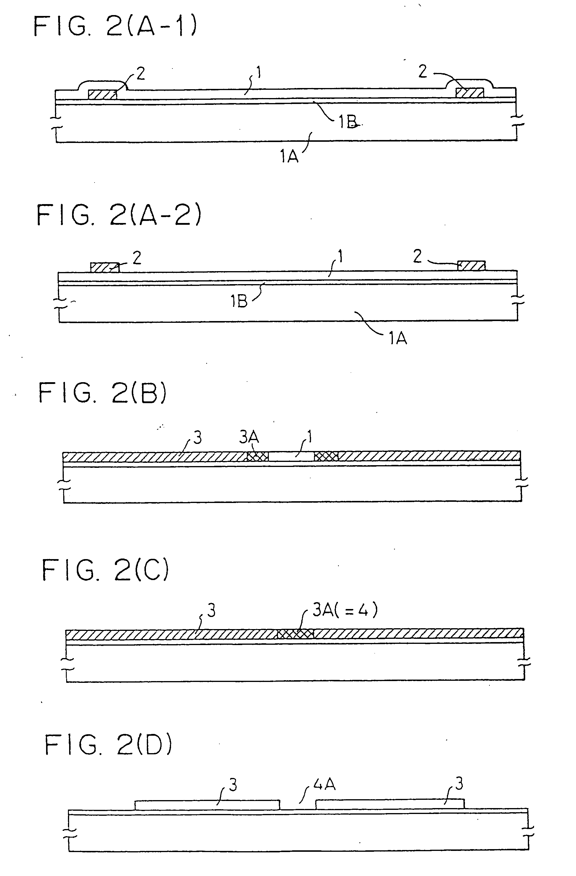
[0071] A method for fabricating a TFT using a crystal silicon film obtained by crystallizing an amorphous silicon film using a plurality of island nickel films formed on Coning 7059 glass substrate as starting points will be described in the present embodiment. There are two methods for forming the island nickel films depending on whether it is formed on or under the amorphous silicon film FIG. 2(A-1) shows the method wherein it is formed under the film and FIG. 2(A-2) shows the method wherein it is formed on the film. What must be careful especially about the later is that because nickel is selectively etched after forming it on the whole surface of the amorphous silicon film in the process, nickel and amorphous silicon react each other and produce nickel silicide, though it is a small amount. Because a good crystalline silicon film which the present invention aims for cannot be obtained if this nickel silicide remains as it is, it is necessary to remove this nickel silicide fully ...

second embodiment

[0090]FIG. 5 shows a case when a TFT for an aluminum gate was fabricated similarly to that shown in FIG. 4. However, the amorphous silicon was used as an active layer in this embodiment: As shown in FIG. 5(A), a ground silicon oxide film 32 was deposited on a substrate 31 and an amorphous silicon film 33 with a thickness of 2000 to 3000 angstrom was deposited further on that. An adequate amount of P type or N type impurities may be mixed in the amorphous silicon film. Then island nickel or nickel silicide coating film 34A and 34B were formed as described above and the amorphous silicon film was crystallized by growing laterally by annealing for 8 hours at 550° C. or for four hours at 600° C. in this state.

[0091] Then a crystal silicon film thus obtained was patterned as shown in FIG. 5(B). At this time, because the silicon film contained a large amount of nickel in the middle in the figure (the intermediate portion between the nickel or nickel silicide film 34A and 34B), the patter...

third embodiment

[0094]FIG. 6 shows a process when a CMOS type TFT was fabricated. As shown in FIG. 6(A), a ground silicon oxide film 52 was deposited on a substrate 51 and an amorphous silicon film 53 with a thickness of 1000 to 1500 angstrom was deposited further on that. Then as described above, island nickel or nickel silicide coating film 54 was formed and annealing was implemented in this state at 550° C. A silicon silicide region 55 moved in the direction of plane, not in the direction of thickness, of the coating film and the crystallization advances by this process. The amorphous silicon film changed into crystal silicon as shown in FIG. 6(B) by four hours of annealing. The silicon silicide regions 59A and 59B were driven away toward the edge along the advancement of the crystallization.

[0095] Then an island silicon region 56 was formed by patterning the crystal silicon film thus obtained as shown in FIG. 6(B) Here, an attention must be paid on that nickel was highly concentrated in the bo...


PUM


Abstract

A method for manufacturing a semiconductor device such as a thin film transistor using a crystal silicon film is provided. The crystal silicon film is obtained by selectively forming films, particles or clusters containing nickel, iron, cobalt, ruthenium, rhodium, paradium, osmium, iridium, platinum, scandium, titanium, vanadium, chrome, manganese, copper, zinc, gold, silver or silicide thereof in a form of island, line, stripe, dot or film on or under an amorphous silicon film and using them as a starting point, by advancing its crystallization by annealing at a temperature lower than a normal crystallization temperature of an amorphous silicon. A transistor whose leak current is low and a transistor in which a mobility is high are obtained in the same time in structuring a dynamic circuit having a thin film transistor by selectively forming a cover film on a semiconductor layer which is to become an active layer of the transistor and by thermally crystallizing it thereafter.

Description

BACKGROUND OF THE INVENTION [0001] 1. Field of the Invention [0002] The present invention relates to a method for fabricating an integrated circuit or more concretely to a semiconductor circuit having a matrix device (including an electro-optic display and semiconductor memory) having a matrix structure and a MOS or MIS (metal-insulator-semiconductor) type field effect element (hereinafter generally referred to as a MOS type element) as a switching element and characterized in its dynamic operation such as a liquid crystal display device and dynamic RAM (DRAM) and a driving circuit therefor or an integrated driving circuit like an image sensor. The present invention particularly relates to a device employing a thin film semiconductor element such as a thin film semiconductor transistor or the like which is formed on an insulating surface as a MOS type element and to a device having a thin film transistor whose active layer is formed by crystal silicon. [0003] 2. Description of the R...

Claims


Application Information

Patent Timeline
IPC IPC(8): H01L21/20H01L21/336H01L21/77H01L21/84
CPCG09G2300/0408H01L21/2022H01L27/1281H01L29/66757H01L27/1277H01L27/1251H01L21/02672H01L21/02532
Inventor ZHANG, HONGYONGUOCHI, HIDEKITAKAYAMA, TORUFUKUNAGA, TAKESHITAKEMURA, YASUHIKO
Owner SEMICON ENERGY LAB CO LTD
Why Eureka
Try Eureka