Integrated underfill process for bumped chip assembly

a chip assembly and integrated technology, applied in the assembly of printed circuits, printed circuit manufacturing, basic electric elements, etc., can solve the problems of significantly shortening the manufacturing cycle and reducing the likelihood of die skewing, so as to increase the weight of the chip or die, minimize the effect of die skewing and high yield

Inactive Publication Date: 2005-02-10
INDIUM CORPORATION
View PDF17 Cites 66 Cited by
  • Summary
  • Abstract
  • Description
  • Claims
  • Application Information

AI Technical Summary

Benefits of technology

[0022] The integrated underfilling process provides a high yield process and void free underfill for the final product. Because a thin layer of unfilled underfill is allowed to flood and flow into the gap between chip and substrate, the underfill material is able to wet any contacted surface and replaces the air space underneath the die with underfill material, avoiding the formation of air bubbles, and assuring that void free underfill is formed during the reflow process. Unlike the wafer-level a

Problems solved by technology

The self-centering force resulting from the molten solder joint further reduces the likelihood of die skewing.
The incorporation of underfilling i

Method used


Image

  • Integrated underfill process for bumped chip assembly
  • Integrated underfill process for bumped chip assembly
  • Integrated underfill process for bumped chip assembly

Examples


Embodiment Construction

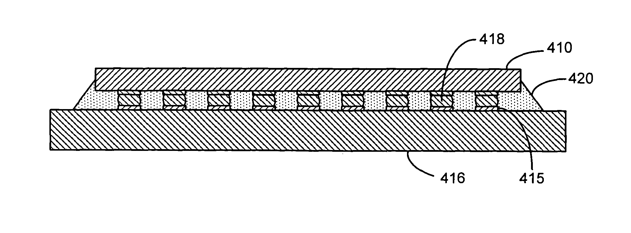
[0033] In accordance with the present invention a method and system for assembling a chip or IC die to a substrate is disclosed. FIG. 4a shows a schematic view of a chip or die 410 with a plurality of conductive bumps 400. The conductive bumps 400 are typically disposed on metallurgical pads 408 disposed on a surface of the chip or die 410. The die 410 may be one of a plurality of dies in wafer. The presently disclosed process may be applied to individual dies, e.g. die-level processes, and to a collection of dies in a wafer, e.g. wafer-level processes. Generally a die 410 has a surface containing metallurgical pads 408 and corresponding chip bumps or contacts 400. The bumps may be of any suitable conductive materials, e.g. eutectic SnPb solders, high Pb solders, lead free solders, Sn and Sn alloy solders, and metals such as Cu, Au, Ag, Ni, Sn, or suitable alloys thereof. Preferably, the chip or IC die bump materials will have a melting point above 100° C. Prior to applying underfil...


PUM

PropertyMeasurementUnit
Percent by massaaaaaaaaaa

Abstract

An integrated underfilling process for attaching a chip/die having conductive solder bump contacts to a substrate. The process involves B-staging filled underfill on the chip/die, depositing a fluxing unfilled underfill onto the surface of the substrate, mating the chip/die with the B-staged underfill to the substrate and reflowing the assembled chip/substrate. The B-staged filled underfill reduces the coefficient of thermal expansion of the underfill fillet and the fluxing unfilled underfill removes metal oxide from the surface of the solder bump contacts and bond pads to promote the formation of reliable metallurgical joints.

Description

CROSS REFERENCE TO RELATED APPLICATIONS [0001] Not Applicable STATEMENT REGARDING FEDERALLY SPONSORED RESEARCH OR DEVELOPMENT [0002] Not Applicable BACKGROUND OF THE INVENTION [0003] The present invention relates to assembly of integrated circuit (“IC”) packages, such as flip chip, chip scale and ball grid array (BGA) packages using underfill. [0004] Flip chip, chip scale package (CSP) and ball grid array (BGA) are various forms of integrated circuit packages. Such packages are designed to meet the demands of the ever-increasing requirements for higher I / O density, miniaturization, and improved electrical performance. [0005] A chip or die is typically mounted on an substrate with interconnect material to form an IC assembly. Due to the large mismatch between the coefficient of thermal expansion (CTE) of silicon chips, laminate boards (i.e., substrate) and solder interconnects, electrical failures associated with the interconnect between the IC and the substrate are relatively common...

Claims


Application Information

Patent Timeline
IPC IPC(8): H01L21/56H01L21/60H01L23/29
CPCH01L21/563H01L23/293H01L23/295H01L24/81H01L2224/13111H01L2224/16225H01L2224/73203H01L2224/73204H01L2224/81801H01L2224/83191H01L2224/83192H01L2224/83193H01L2224/83856H01L2924/01005H01L2924/01013H01L2924/01029H01L2924/01047H01L2924/0105H01L2924/01077H01L2924/01079H01L2924/01082H01L2924/01322H01L2924/09701H01L2924/14H01L2924/01006H01L2924/01033H01L2924/01087H01L2924/014H01L24/29H01L2224/32225H01L2924/0132H01L2924/157H01L2924/15787H01L2924/15788H01L2924/1579H01L24/83H01L2224/73104H01L2224/29111H01L2224/2919H01L2924/10253H01L2224/81191H01L2224/83862H01L2224/83868H01L2224/83885Y10T29/49146Y10T29/4913Y10T29/49144H01L2924/00H01L2924/3512H01L2924/00014H01L2224/05568H01L2224/05573H01L2924/12042H01L2224/05599
Inventor YIN, WUSHINGLEE, NING-CHENG
Owner INDIUM CORPORATION
Why Eureka
Try Eureka