

Ceramic substrate, ceramic heater, electrostatic chuck and wafer prober for use in semiconductor producing and inspecting devices
a ceramic heater and ceramic substrate technology, applied in the direction of ohmic-resistance heating, hot plate heating arrangement, semiconductor/solid-state device testing/measurement, etc., to achieve the effect of reducing the insulation resistance and reducing the deposition of ceramic particles thereon
- Summary
- Abstract
- Description
- Claims
- Application Information
AI Technical Summary
Benefits of technology
Problems solved by technology
Method used
Image

Examples
example of synthesis
Synthesis of Aluminum Nitride
[0199][0199] (1) A porous γ-Fe2O3 powder with a mean particle diameter of 3 μm was impregnated with a 10 weight % ethanolic solution of titanium isopropoxide containing 0.5 weight % of HCl and allowed to stand for hydrolysis at 25° C. for 24 hours to provide a U / Th adsorbent. [0200] (2) In a Teflon vessel, 1000 weight parts of pulverized bauxite was mixed with a 10% aqueous solution of sodium hydroxide, and the mixture was treated in an autoclave at 190° C. for 5 hours. The reddish sludge was filtered off to recover an aqueous solution of sodium aluminate. [0201] (3) This aqueous solution of sodium aluminate was adjusted to pH 12 with 1N-HCl and the above adsorbent was dispersed therein at 50° C. for 0.5 hour under vibration. Similarly, dispersions kept under vibration for 1, 2, 3, 4, 5 and 6 hours were prepared. Thus, a total of 7 kinds of dispersions were provided. [0202] (4) The adsorbent was filtered off and the filtrate was adjusted to pH 8.5 with ...
example 1
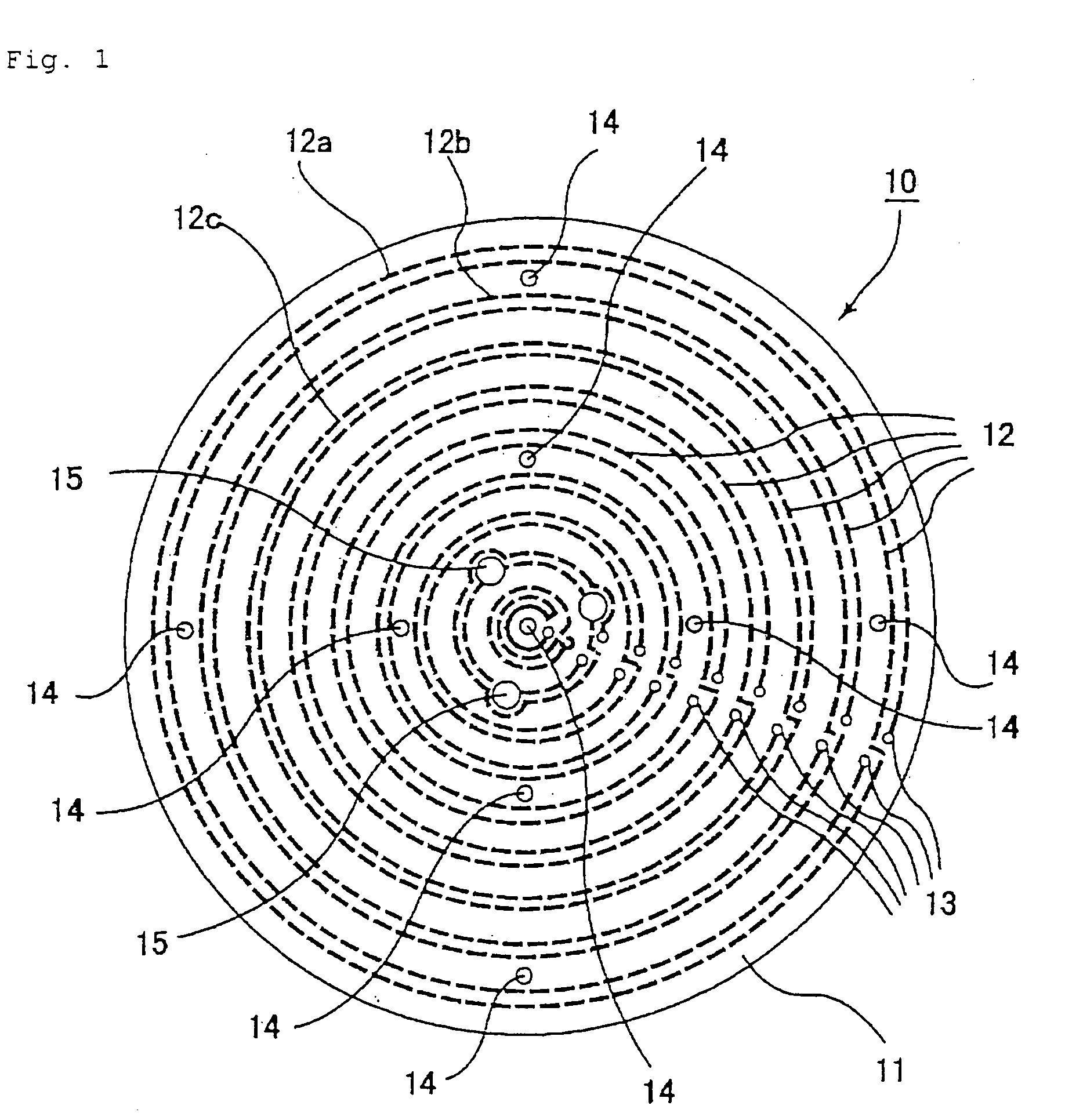
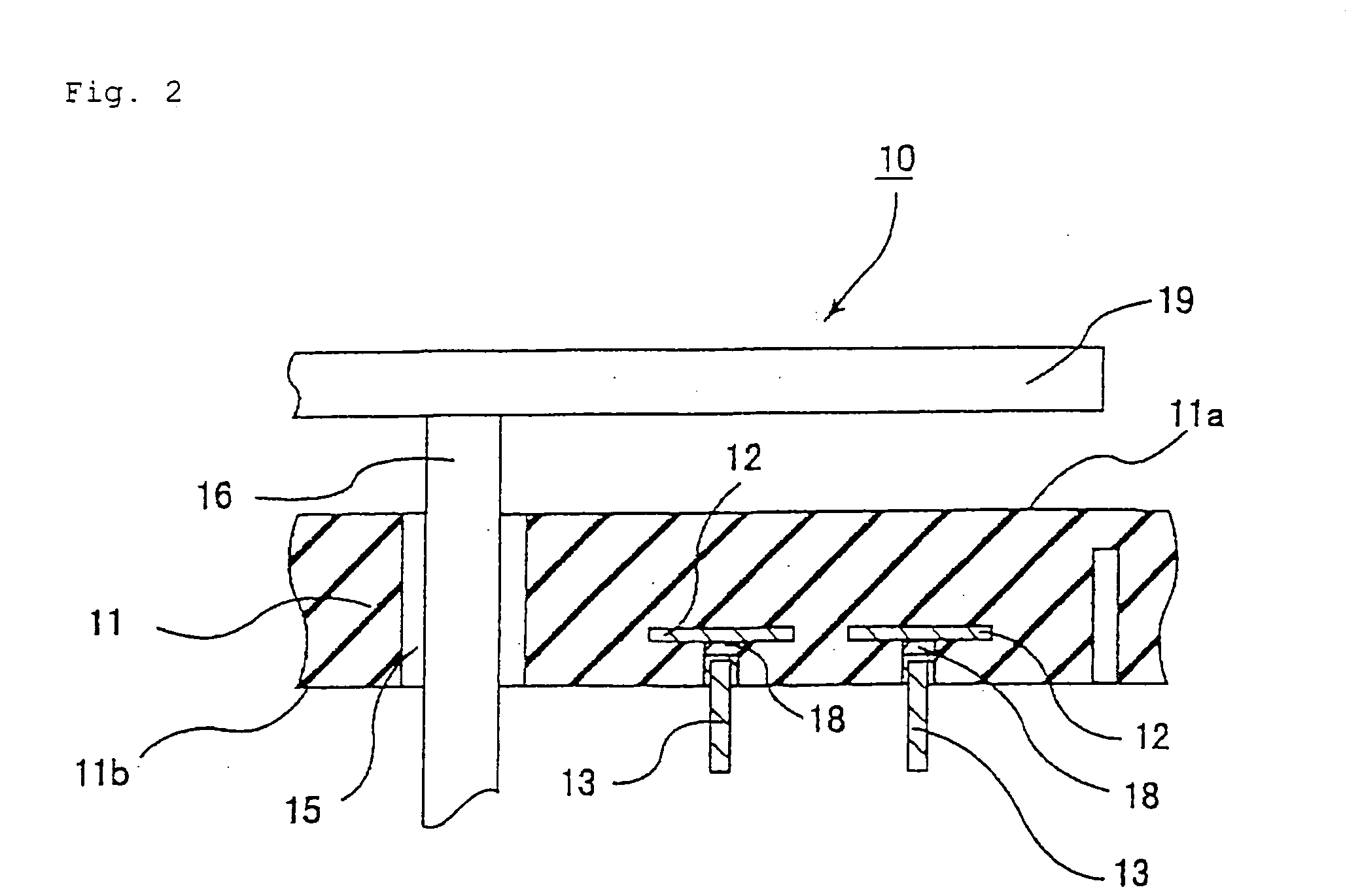
Manufacture of a Ceramic Heater Having a Heating Element on its Surface
[0206][0206] (1) A composition comprising 100 weight parts of any of said aluminum nitride powders A to G having a mean particle diameter of 1.1 μm, 4 weight parts of yttria (mean particle dia.: 0.4 μm), 12 weight parts of acrylic binder and the balance of alcohol was spray-dried to prepare a granular powder. [0207] (2) This granular powder was set in a metal mold and formed into a raw formed body. [0208] (3) The raw formed body was then hot-pressed at 1800° C. and 200 kg / cm2 to provide a 3 mm-thick aluminum nitride board.
[0209] From this board, a disk having a diameter of 210 mm was cut out to provide a ceramic disk (heater plate). This plate was drilled to form apertures corresponding to the through holes for accepting support pins for supporting a semiconductor wafer and cavities corresponding to the bottomed holes for embedding thermocouples (diameter: 1.1 mm, depth: 2 mm). [0210] (4) On the heater plate pr...
example 2
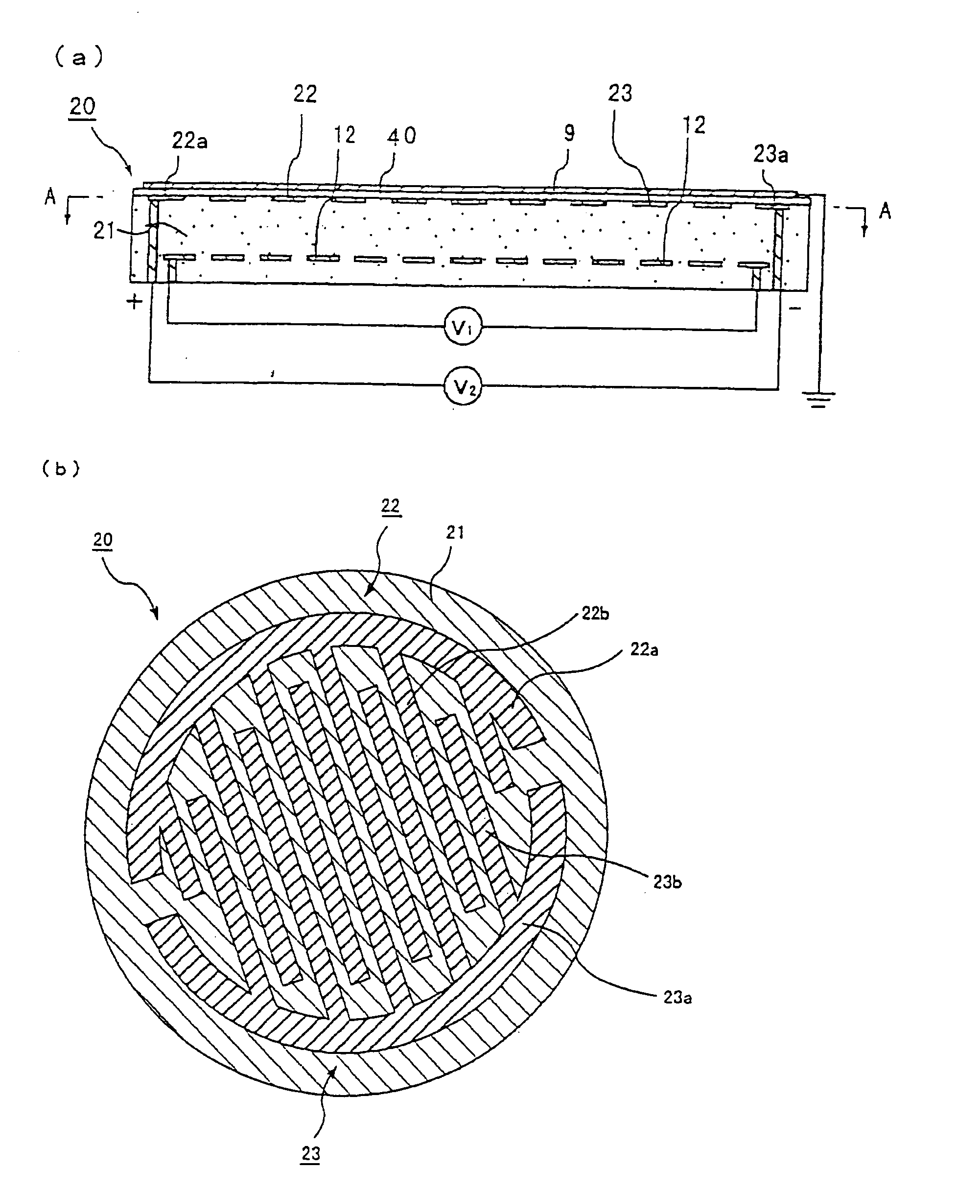
Manufacture of an Electrostatic Chuck Internally Provided with a Heating Element and Static Electrodes
[0218][0218] (1) A paste was prepared by compounding 100 weight parts of any of said aluminum nitride powders A to G with 4 weight parts of yttria (average particle diameter: 0.4 μm), 11.5 weight parts of acrylic binder, 0.5 weight part of dispersant and 53 weight parts of alcohol (1-butanol and ethanol), and using the paste a 0.47 mm-thick green sheet was molded by the doctor blade method. [0219] (2) This green sheet was dried at 80° C. for 5 hours and punched to form through holes 15 serving as semiconductor wafer-support pin-accepting holes, 1.8 mm, 3.0 mm and 5.0 mm in diameter, and those serving as conductor-filled through holes 18 for electrical connection to external terminals. [0220] (3) A conductor containing paste A was prepared by compounding 100 weight parts of a tungsten carbide powder having a mean particle diameter of 1 μm, 3.0 weight parts of acrylic binder, 3.5 wei...
PUM
| Property | Measurement | Unit |
|---|---|---|
| thick | aaaaa | aaaaa |
| thickness | aaaaa | aaaaa |
| thickness | aaaaa | aaaaa |
Abstract
Description
Claims
Application Information