Group III nitride compound semiconductor laser

a semiconductor laser and nitride technology, applied in the direction of lasers, semiconductor devices, semiconductor lasers, etc., can solve the problems of not being easy for all the semiconductor lasers, and achieve the effect of easy control of the thickness of the cladding layer and easy manufacturing process

Inactive Publication Date: 2005-02-10
TOYODA GOSEI CO LTD
View PDF6 Cites 32 Cited by
  • Summary
  • Abstract
  • Description
  • Claims
  • Application Information

AI Technical Summary

Benefits of technology

[0018] By forming the third layer having larger aluminum (Al) composition in group III elements compared with that of the second layer between the first layer which functions as a guide layer and actually confines carriers to an active layer functioning as a main layer to oscillate laser and the second layer which mainly confine light to the active layer which functions as a main layer oscillating laser and the first layer, the third layer can protect the first layer in an etching process. That is because etching rate of a group III nitride compound semiconductor becomes smaller in proportion as the aluminum (Al) composition increases, there are some time during etching the third layer. Accordingly, in a process of forming a ridged carrier injection part, a guide layer cannot be damaged even when the production is not uniform. Or because the third layer having larger aluminum (Al) composition of group III elements compared with the second layer is formed between the

Problems solved by technology

When forming the ridged hole injection part B, however, it is not easy for all the semiconductor lasers formed on a wafer that a boundary between

Method used


Image

  • Group III nitride compound semiconductor laser
  • Group III nitride compound semiconductor laser
  • Group III nitride compound semiconductor laser

Examples


Embodiment Construction

[0026] The present invention will next be described in detail with reference to embodiments, which should not be construed as limiting the invention thereto.

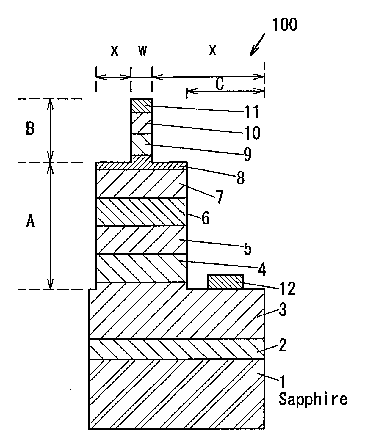
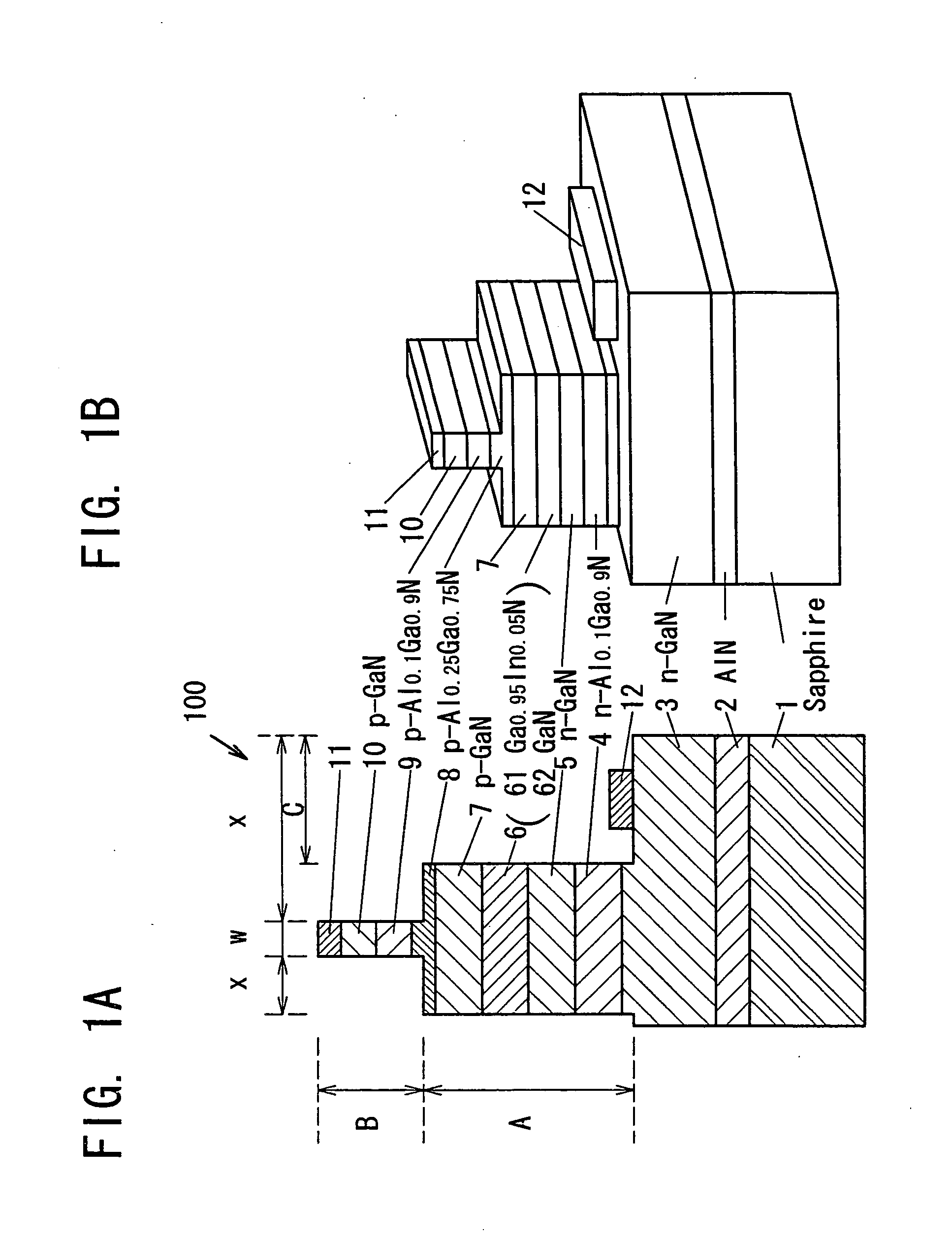
[0027]FIG. 1A illustrates a sectional view of a semiconductor laser 100. FIG. 1B illustrates a view showing a structure of the semiconductor laser 100.

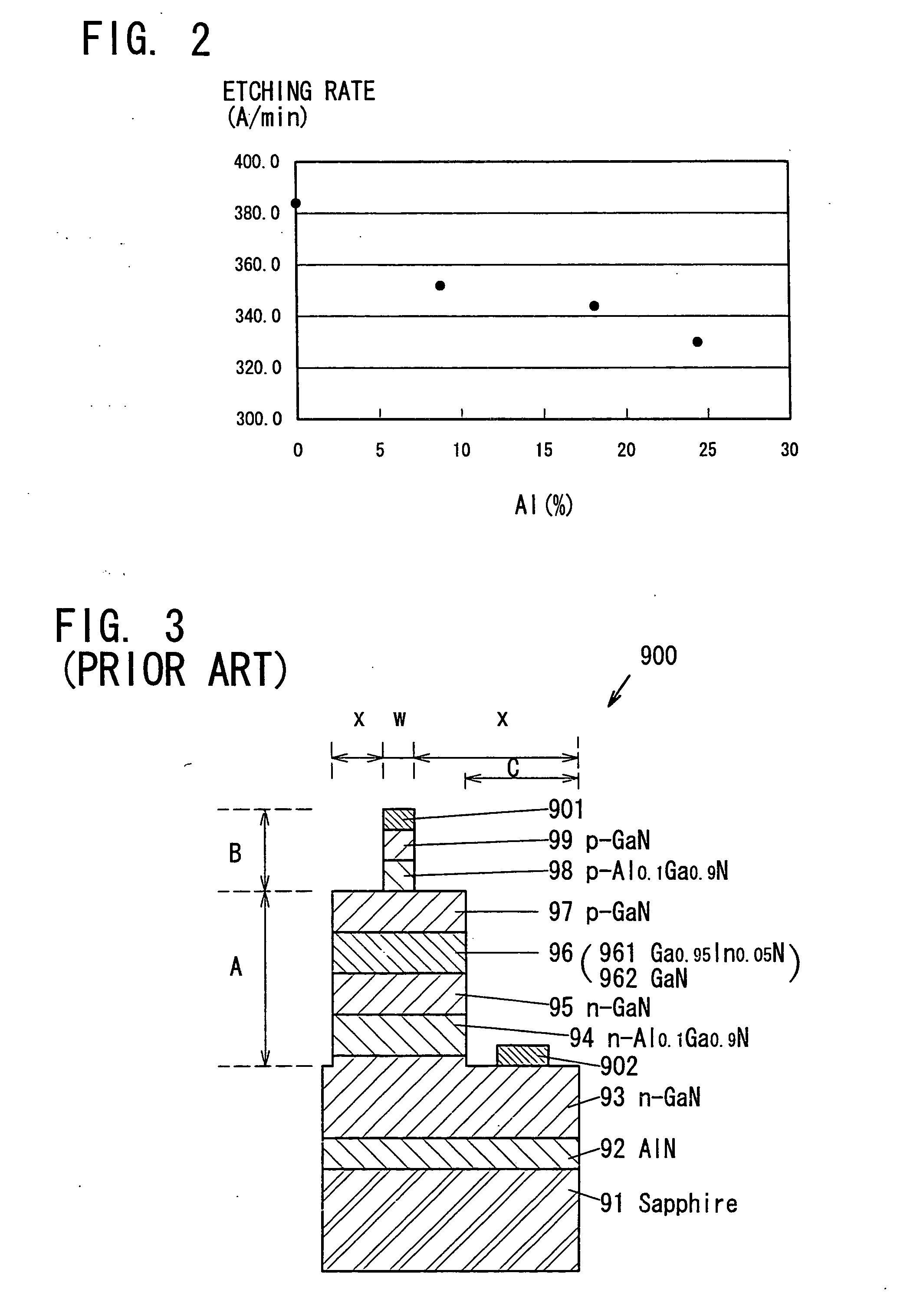
[0028] The semiconductor laser 100 has a sapphire substrate 1, and an AlN buffer layer 2 having a thickness of 50 nm is formed on the substrate 1. Alternatively, the buffer layer 2 can be made of GaN, GaInN or AlGaN. On the buffer layer 2, the following layers are formed consecutively: about 4.0 μm in thickness of silicon (Si) doped gallium nitride (GaN) n-layer 3, having an electron concentration of 1×10¹⁸ / cm−3; 500 nm in thickness of Si-doped Al0.1Ga0.9N n-cladding layer 4, having an electron concentration of 1×10¹⁸ / cm−3; 100 nm in thickness of Si-doped GaN n-guide layer 5, having an electron concentration of 1×10¹⁸ / cm−3; and an active layer 6 having multiple quantum well (MQW...


PUM


Abstract

A semiconductor laser comprises a sapphire substrate, an AlN buffer layer, Si-doped GaN n-layer, Si-doped Al0.1Ga0.9N n-cladding layer, Si-doped GaN n-guide layer, an active layer having multiple quantum well (MQW) structure in which about 35 Å in thickness of GaN barrier layer 62 and about 35 Å in thickness of Ga0.95In0.05N well layer 61 are laminated alternately, Mg-doped GaN p-guide layer, Mg-doped Al0.25Ga0.75N p-layer, Mg-doped Al0.1Ga0.9N p-cladding layer, and Mg-doped GaN p-contact layer are formed successively thereon. A ridged hole injection part B which contacts to a ridged laser cavity part A is formed to have the same width as the width w of an Ni electrode. Because the p-layer has a larger aluminum composition, etching rate becomes smaller and that can prevent from damaging the p-guide layer in this etching process.

Description

[0001] This is a patent application based on Japanese patent applications No. 2002-063811 and No. 2003-040462, which were filed on Mar. 8, 2002 and Feb. 19, 2003, respectively, and which are incorporated herein by reference. BACKGROUND OF THE INVENTION [0002] 1. Field of the Invention [0003] The present invention relates to a group III nitride compound semiconductor laser. Especially, the present invention relates to a group III nitride compound semiconductor laser having a ridge type of a resonator. [0004] 2. Description of the Related Art [0005] A semiconductor laser which has a cladding layer and an active layer and so on made of a group III nitride compound semiconductor (AlxGayIn1-x-yN, 0≦x≦1, 0≦y≦1 and 0≦x+y≦1) has been known. The conventional semiconductor laser is a semiconductor diode having multi-layer structure with multiple group III nitride compound semiconductor layers, which are formed on a sapphire substrate in sequence. A conventional example of the semiconductor di...

Claims


Application Information

Patent Timeline
IPC IPC(8): H01S5/20H01S5/042H01S5/22H01S5/227H01S5/323H01S5/343
CPCB82Y20/00H01S5/2004H01S2301/18H01S5/22H01S5/34333H01S5/209H01S5/30
Inventor HATANO, TAKASHIIWAYAMA, SHOKOIKE, MASAYOSHI
Owner TOYODA GOSEI CO LTD
Why Eureka
Try Eureka