Manufacturing method for semiconductor device, semiconductor device and semiconductor wafer

a manufacturing method and semiconductor technology, applied in the direction of crystal growth process, polycrystalline material growth, chemically reactive gas, etc., can solve the problems of reducing light-emitting efficiency, limiting the combination of base and growth layer, and generating cracks on the growth layer. , to achieve the effect of preventing crack generation and high yield

Active Publication Date: 2005-02-24
PANASONIC CORP
View PDF3 Cites 37 Cited by
  • Summary
  • Abstract
  • Description
  • Claims
  • Application Information

AI Technical Summary

Benefits of technology

[0010] Considering the problems mentioned above, it is an object of the present invention to provide, even when a semiconductor layer grows as much as causing a distortion larger than a destruction limit, a manufacturing method for a semiconductor device capable of moderating an influence of a crack and forming a semiconductor device with a high yield, and a manufacturing method for a semiconductor device and a semiconductor substrate that can preventing the crack generation.

Problems solved by technology

When such distortion is deposited and a limit is reached, a crack is generated on the growth layer.
Also, there is a limitation for a combination of the base and the growth layer.
Furthermore, in the case where a semiconductor material with a film hetero-structure using InGaN is applied to a light-emitting device with a short wavelength such as a purple light to an ultraviolet radiation, an InGaN layer works as a light absorption layer so that a light-emitting efficiency remarkably declines and an high-efficient semiconductor device cannot be acquired.

Method used


Image

  • Manufacturing method for semiconductor device, semiconductor device and semiconductor wafer
  • Manufacturing method for semiconductor device, semiconductor device and semiconductor wafer
  • Manufacturing method for semiconductor device, semiconductor device and semiconductor wafer

Examples


first embodiment

[0042] (First Embodiment)

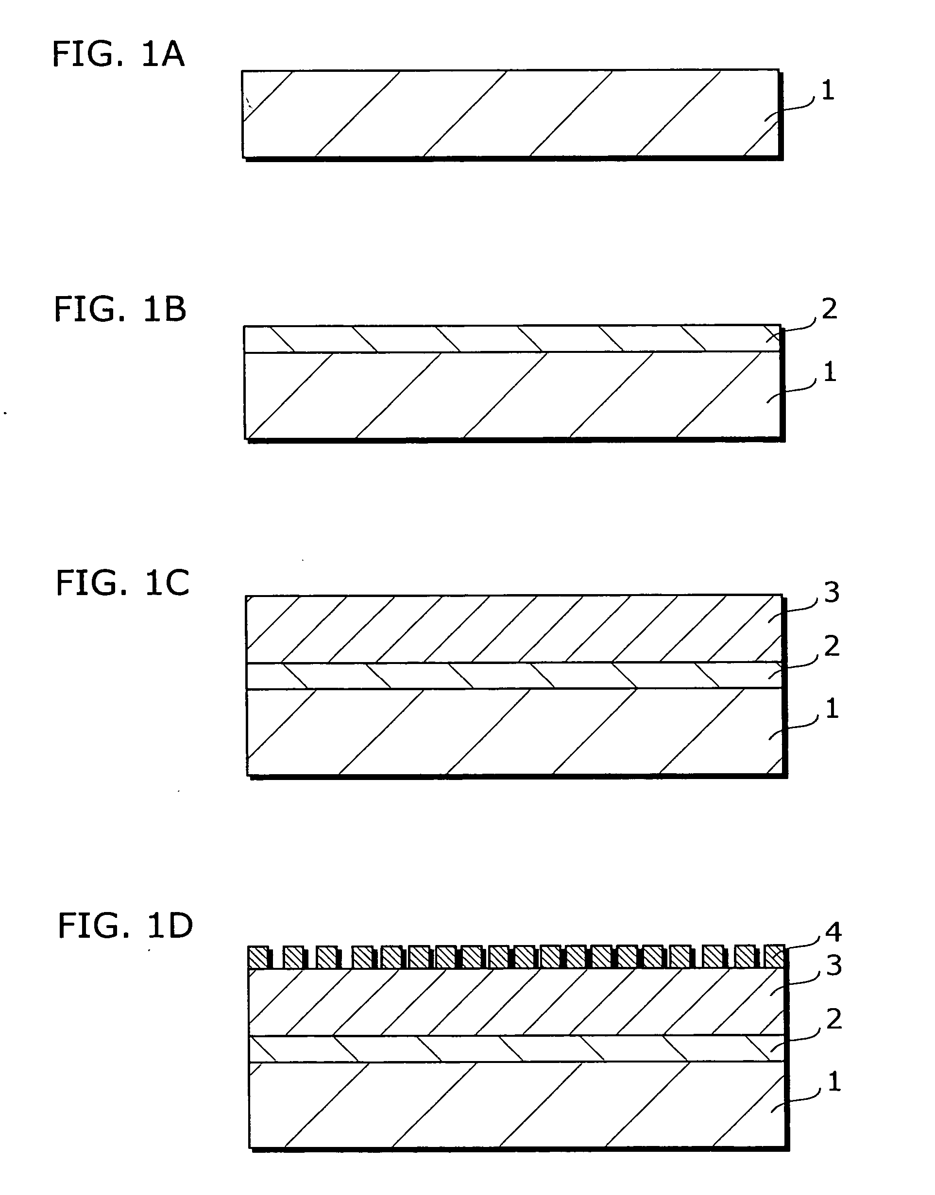
[0043] By referring to FIGS. 1 to 7, a manufacturing method for an ultraviolet emitting LED device 20 (refer to following FIG. 3J) in the first embodiment is explained. Here, FIGS. 1 to 3 show a process of the manufacturing method for the ultraviolet LED device 20 in the present embodiment using cross-section diagrams. A substrate 1 shown in FIG. 1A is a n-type 6HSiC whose diameter is 2 inch.

[0044] Firstly, an AlN layer 2 is formed in 1 μm thick at a high temperature of 1000° C. on the substrate 1 by a Metal Organic Chemical Vapor Deposition (MOCVD) method using trimethyl aluminum as a III group material, ammonia as a V group material, and hydrogen as a carrier gas (FIG. 1B).

[0045] Following that, on the AlN layer 2, a base layer 3 made of n-type Al0.2Ga0.8N is formed in 2 μm thick at a high temperature of 1000° C. (FIG. 1C). Here, AlGaN can be obtained by mixing trimethyl gallium with trimethyl aluminum in an appropriate proportion and growing the mixed. ...

second embodiment

[0098] (Second Embodiment)

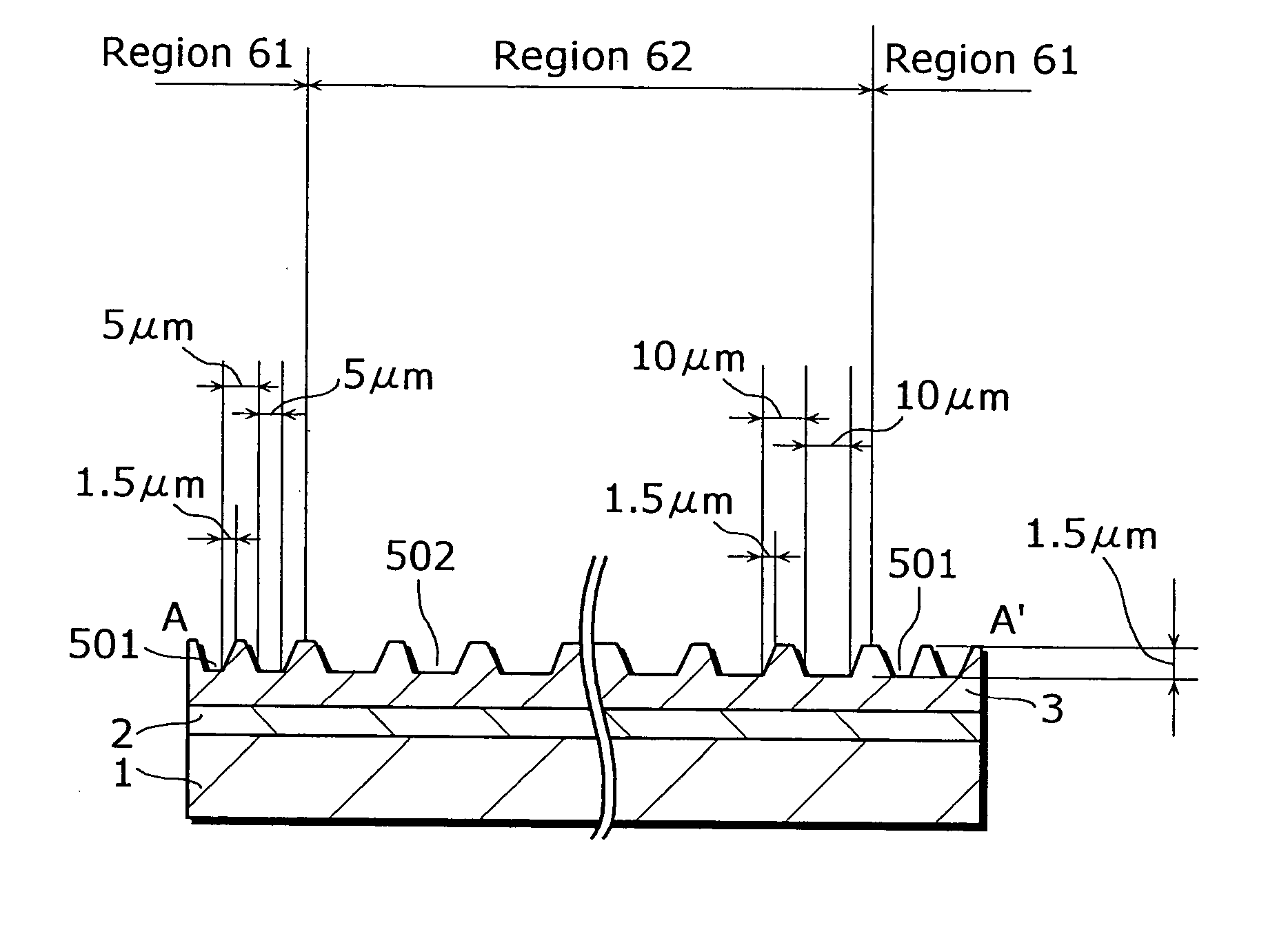
[0099] By referring to FIGS. 8 to 14, a manufacturing method for the ultraviolet LED device 30 (refer to FIG. 10J) in the second embodiment is explained. In the present embodiment, an example which is effective for the crack prevention without forming steps for low defectives in the device region 61 is explained.

[0100]FIG. 8A is a cross-section diagram of the substrate 1.

[0101] On the substrate 1 made of the n-type 6HSiC, the AlN layer 2 is formed to have a thickness of 1 μm by the MOCVD method (FIG. 8B).

[0102] Next, on the AlN layer 2, the base layer3 made of the n-type Al02Ga0.8N is formed to have a thickness of 2 μm (FIG. 8C).

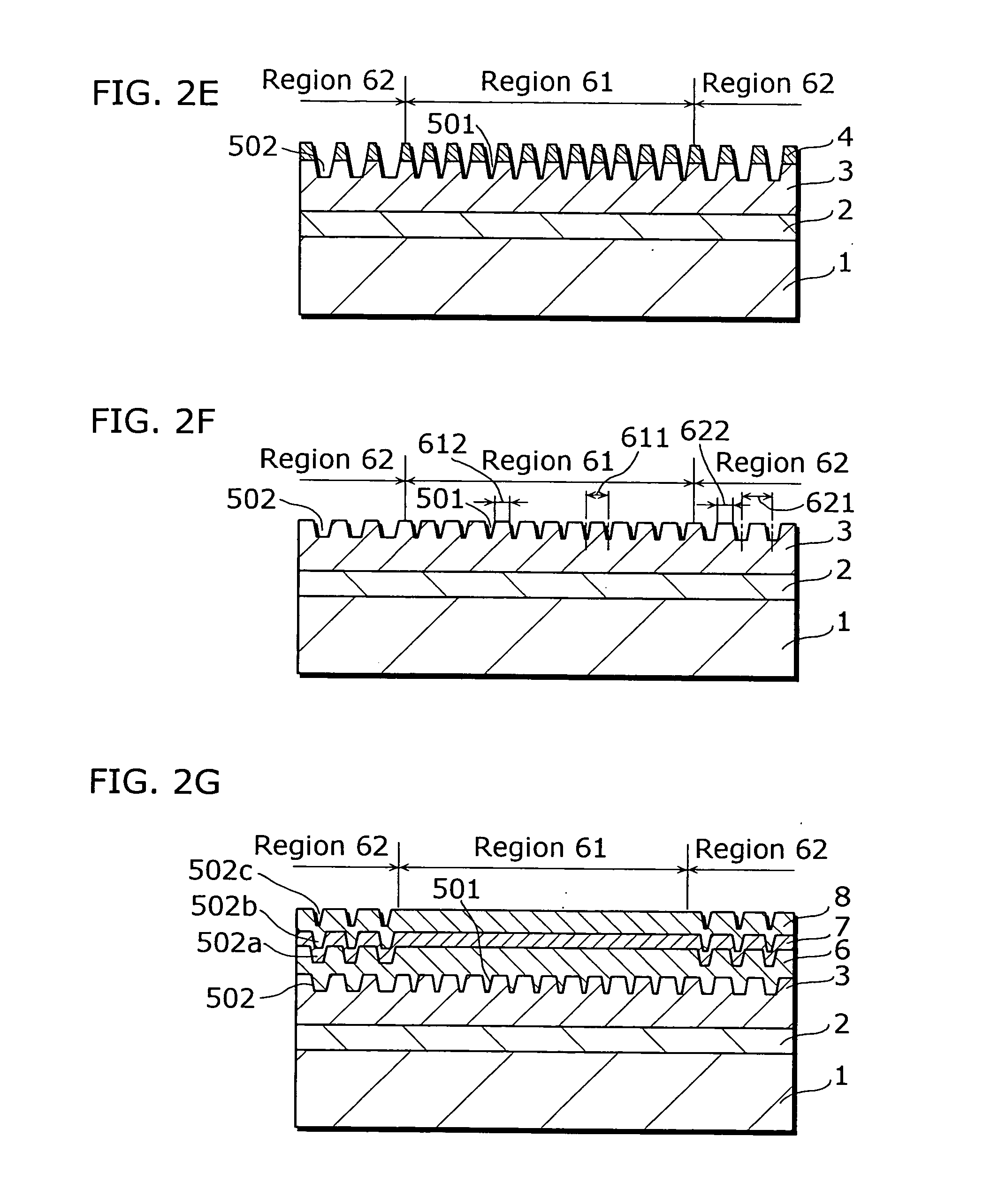
[0103] As shown in FIG. 8D, the masks 4 are formed on the base layer 3 by the photoresist. The mask pattern is patterned to cover all regions except where the trenches 502 are formed and steps are not set intentionally in the device region 61, the trenches 502 being discussed later.

[0104] Further, the trenches 502 are formed by...

third embodiment

[0121] (Third Embodiment)

[0122] The present embodiment shows an example examined for plane shapes of trenches. Hereafter, a manufacturing method for an ultraviolet LED device 40 (not shown in diagrams) in the present embodiment is explained with reference to FIG. 15 and FIG. 16.

[0123]FIGS. 15 and 16 are diagrams showing shapes of trenches to be examined about shapes of a device region 61, a trench region 64 and a convex region 65. Each trench is formed using the exactly same manufacturing method used in the first embodiment (that is, only the shape of the trench 502 shown in FIG. 2F is changed). The trench region 64 shown in FIGS. 15 and 16 applies to the second trench 502 shown in FIG. 2F. The convex region 65 applies to a non-etched region between adjacent second trenches 502 shown in FIG. 2F.

[0124]FIGS. 15A to 15E show examples of shapes of trenches which are effective to prevent a crack generation, that is, shapes of trenches by which the crack is not generated in the device r...


PUM

PropertyMeasurementUnit
diameteraaaaaaaaaa
temperatureaaaaaaaaaa
thickaaaaaaaaaa

Abstract

A manufacturing method for a semiconductor device formed in a device region composed of a plurality of semiconductor layers on a substrate, the method including a trench forming step of forming a trench on the substrate around the device region and a semiconductor growth step of growing the semiconductor layer in the device region.

Description

BACKGROUND OF THE INVENTION [0001] (1) Field of the Invention [0002] The present invention relates to a manufacturing method for a semiconductor device, in particular to a manufacturing method for a III group nitride semiconductor device having heterojunction, such as a light emitting diode (hereafter referred to as LED) in a visible range to an ultraviolet range, a semiconductor laser in a visible range to an ultraviolet range, or a high-speed transistor, and relates to a semiconductor device and a semiconductor wafer manufactured by the III group nitride semiconductor having the heterojunction. [0003] (2) Description of the Related Art [0004] The III group nitride semiconductor made of GaN, InN, AlN or an alloy composed predominantly of these materials is a semiconductor material that can form a hetero-structure of a wide band-gap having an energy gap corresponding to a wave range from a visible light to an ultraviolet radiation. Therefore, it is a preferred material for a LED, a ...

Claims


Application Information

Patent Timeline
Patent Type & Authority Applications(United States)
IPC IPC(8): C30B25/02C30B25/18C30B29/40H01L21/20H01L29/06H01L33/00
CPCC30B25/02C30B25/18C30B29/40H01L21/0237H01L21/02378H01L33/007H01L21/02458H01L21/0254H01L21/02658H01L29/0657H01L21/0243
Inventor ISHIDA, MASAHIRO
Owner PANASONIC CORP
Why Eureka
Try Eureka