Copper-faced modules, imprinted copper circuits, and their application to supercomputers

Inactive Publication Date: 2005-02-24
SALMON TECH
View PDF99 Cites 51 Cited by
  • Summary
  • Abstract
  • Description
  • Claims
  • Application Information

AI Technical Summary

Benefits of technology

[0017] The purpose of the epoxy under layer between chip and board is to prevent mechanical failure such as cracking that can arise from stresses accompanying temperature excursions that occur during manufacturing or operation. Part of the justification for eliminating this under layer in the proposed flip chip mounting structure is that the preferred arrangement of gold stud bumps inserted into wells filled with solder is mechanically stronger (shear forces can not easily detach a stud bump from its pad or a well from its pad). Because the stud bumps are formed from gold, and because gold is one of the

Problems solved by technology

Moisture uptake is critical because small amounts of absorbed water can substantially raise the effective dielectric constant, and a higher dielectric constant may effectively prohibit high frequency operation.
A fabrication facility to process silicon wafers by this method typically costs more than US$1 B today.
There have been two major impediments to the integration of large systems that are exclusively or primarily assembled using flip chip assembly methods: the inability to effectively test such a system (particularly a functional test at full system speed), and the inability to rework defecti

Method used


Image

  • Copper-faced modules, imprinted copper circuits, and their application to supercomputers
  • Copper-faced modules, imprinted copper circuits, and their application to supercomputers
  • Copper-faced modules, imprinted copper circuits, and their application to supercomputers

Examples


Embodiment Construction

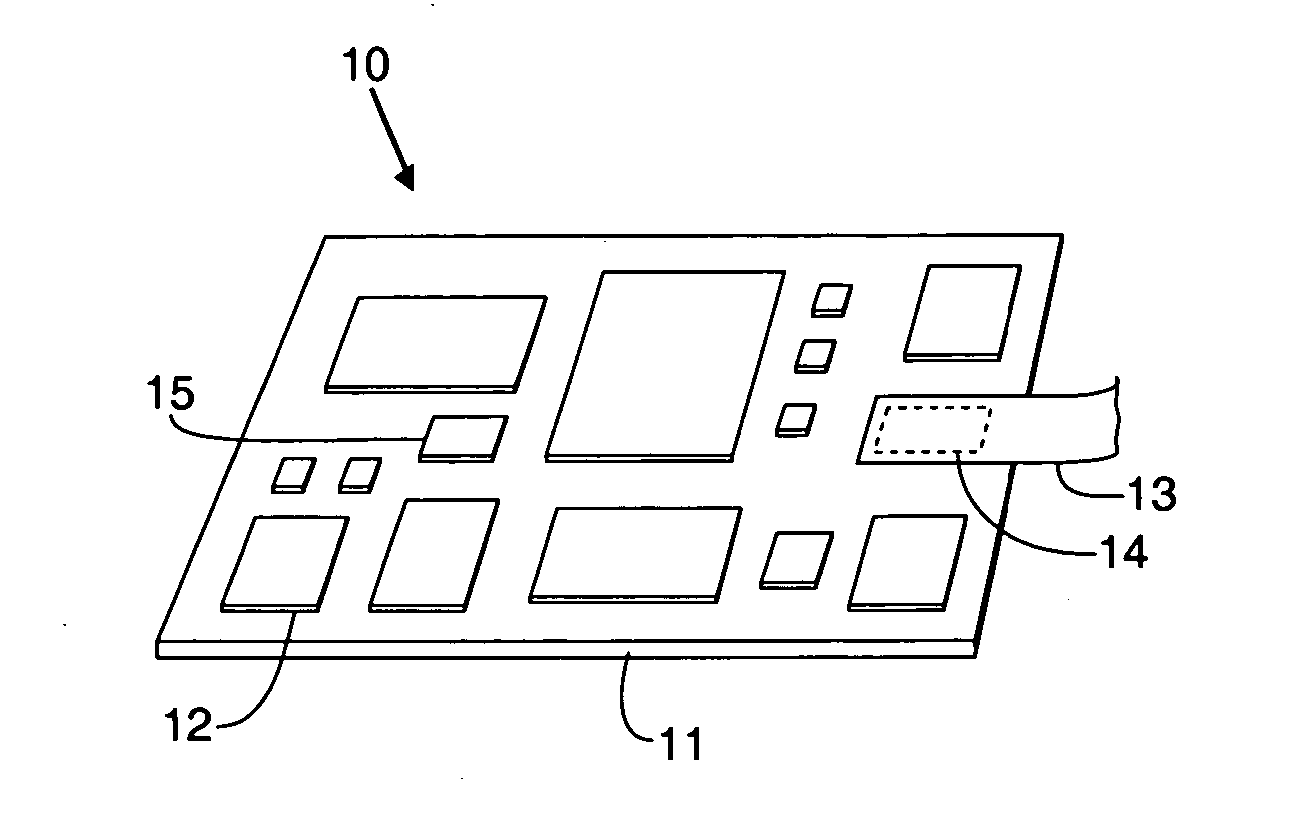
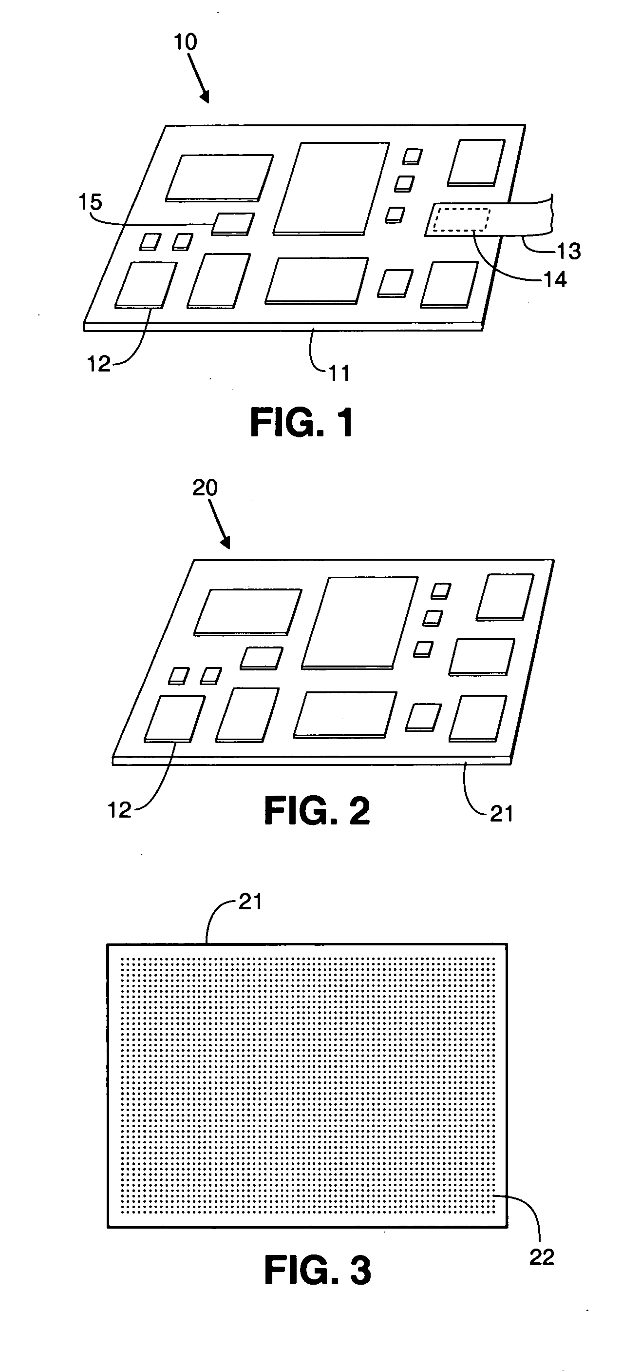
[0065]FIG. 1 shows an electronic module 10 having a conductive substrate 11. (base layer), and multiple integrated circuit chips (IC chips) such as 12 flip chip mounted thereon. Module 10 receives power and communicates with other electronic systems via module access cable 13, utilizing module access port 14, as will be further described. The attachment of IC chips 12 and access cable 13 preferably employ a new version of flip chip assembly wherein each input / output pad of each chip and each cable preferably has a stud bump attached, and each stud bump mates with a well filled with solder formed on top of the interconnection circuit (not shown) fabricated on substrate 11. Detailed manufacturing steps for fabricating these circuits will be described. IC chip 15 may be a test chip, as will be further described. The material of conductive substrate 11 is preferably copper or a dispersion-strengthened copper (DSC). FIG. 1 is an example of a module with a single conductive face.

[0066]FI...


PUM

PropertyMeasurementUnit
Lengthaaaaaaaaaa
Lengthaaaaaaaaaa
Electrical conductivityaaaaaaaaaa

Abstract

A method for fabricating copper-faced electronic modules is described. These modules are mechanically robust, thermally accessible for cooling purposes, and capable of supporting high power circuits, including operation at 10 GHz and above. An imprinting method is described for patterning the copper layers of the interconnection circuit, including a variation of the imprinting method to create a special assembly layer having wells filled with solder. The flip chip assembly method comprising stud bumps inserted into wells enables unlimited rework of defective chips. The methods can be applied to multi chip modules that may be connected to other electronic systems or subsystems using feeds through the copper substrate, using a new type of module access cable, or by wireless means. The top copper plate can be replaced with a chamber containing circulating cooling fluid for aggressive cooling that may be required for servers and supercomputers. Application of these methods to create a liquid cooled supercomputer is described.

Description

RELATED APPLICATIONS [0001] This application claims priority to provisional Application Ser. No. 60 / 496,948 filed Aug. 20, 2003.BRIEF DESCRIPTION OF THE INVENTION [0002] This invention relates to apparatus and method for building microelectronic modules having one or two conductive faceplates, imprinting methods, and their application to blade servers and supercomputers. BACKGROUND OF THE INVENTION [0003] Conventional printed circuit boards are constructed using copper signal planes laminated between glass-epoxy layers. Copper planes (foils) are also used for ground and for power supply voltages. For conventional epoxy laminate boards, trace and space dimensions are typically 100 microns each for a trace pitch of 200 microns, and hole diameters for plated through holes are typically 340 microns or more. More advanced boards are available from companies such as Unitive, Inc. of Research Triangle Park, N.C., USA. Unitive's boards employ BCB, a spin-on resin available from Dow Chemical...

Claims


Application Information

Patent Timeline
IPC IPC(8): H01L21/48H05K1/05H05K3/00H05K3/10H05K3/38H05K3/42H05K3/44H05K3/46
CPCH01L21/486H01L2224/16H01L2924/10253H01L2924/01077H01L2924/01078H01L2924/01079H01L2924/3011H05K1/056H05K3/005H05K3/107H05K3/388H05K3/423H05K3/445H05K3/4608H05K3/465H05K2201/0141H05K2201/09563H05K2203/0108H01L2924/01322H01L2924/00
Inventor SALMON, PETER C.
Owner SALMON TECH
Why Eureka
Try Eureka