

High-frequency semiconductor device
- Summary
- Abstract
- Description
- Claims
- Application Information
AI Technical Summary
Benefits of technology
Problems solved by technology
Method used
Image

Examples
first embodiment
[0031] First Embodiment
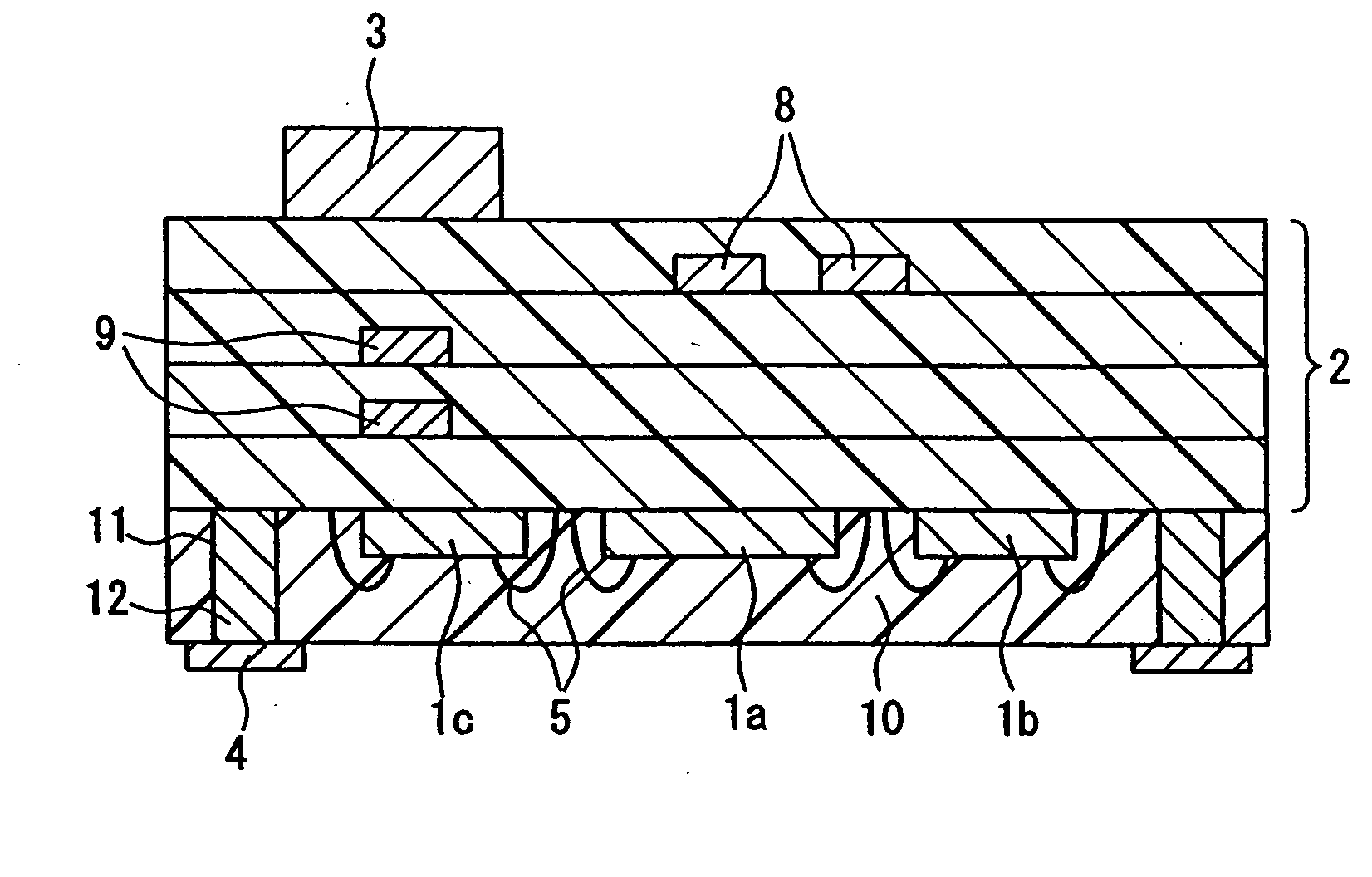
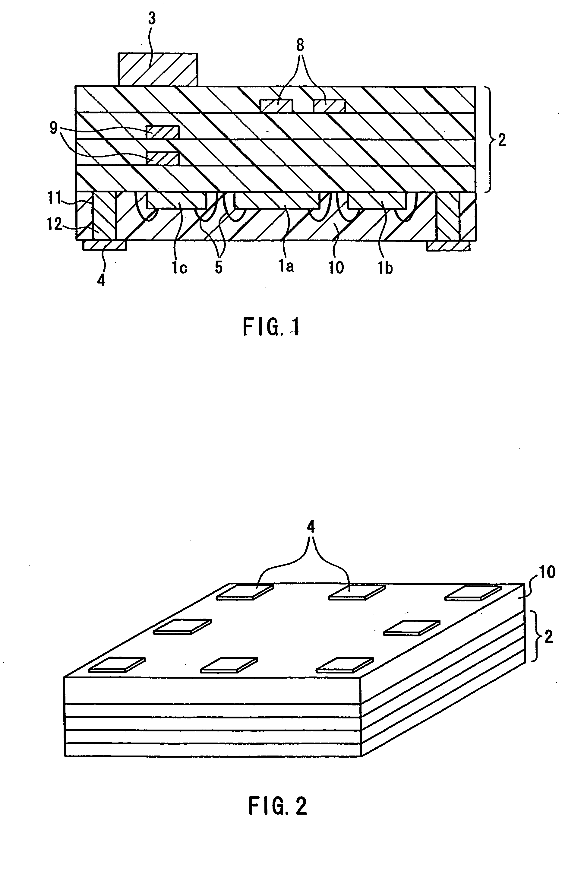
[0032]FIG. 1 is a cross-sectional view of a high-frequency semiconductor device according to Embodiment 1 of the present invention. FIG. 2 is a perspective view of the high-frequency semiconductor device of FIG. 1 seen from its rear side.
[0033] In FIG. 1, the numeral 1a denotes a gallium-arsenide power semiconductor element serving as a power amplifier, 1b denotes a gallium-arsenide semiconductor element serving as a switching element, and 1c denotes a silicon semiconductor element for circuit control. Numeral 2 denotes a non-shrinkage ceramic multilayer substrate, which incorporates in its inner layers printed resistors 8 and printed capacitors 9 formed by printing a paste material that includes metal, and which may be formed by baking at a low temperature. Numeral 3 denotes a chip component such as, for example, a chip capacitor for fine-tuning the high-frequency circuit constants. Numeral 5 denotes metal wires, and 10 denotes a composite resin material lay...
embodiment 2
[0046] Embodiment 2
[0047] Embodiment 2 of the present invention is described with reference to the cross-sectional view of the high-frequency semiconductor device shown in FIG. 3.
[0048] The device of FIG. 3 differs from that according to Embodiment 1 shown in FIG. 1 in that the gallium-arsenide power semiconductor element 1a, the gallium-arsenide semiconductor element 1b, and the silicon semiconductor element 1c are flip-chip connected on the circuit pattern on the bottom surface of the ceramic multilayer substrate 2 via bumps 13 having a metal core.
[0049] The bumps 13 are formed through SBB (stud ball bonding) using gold wire, and maintain a gap of approximately 40 μm between the semiconductor elements 1a, 1b, and 1c and the ceramic multilayer substrate 2. Other techniques that can be employed to provide the bumps 13 include a technique employing plating around a copper core material serving as the core and adhering with a conductive resin, a technique employing an ACF (anisotrop...
embodiment 3
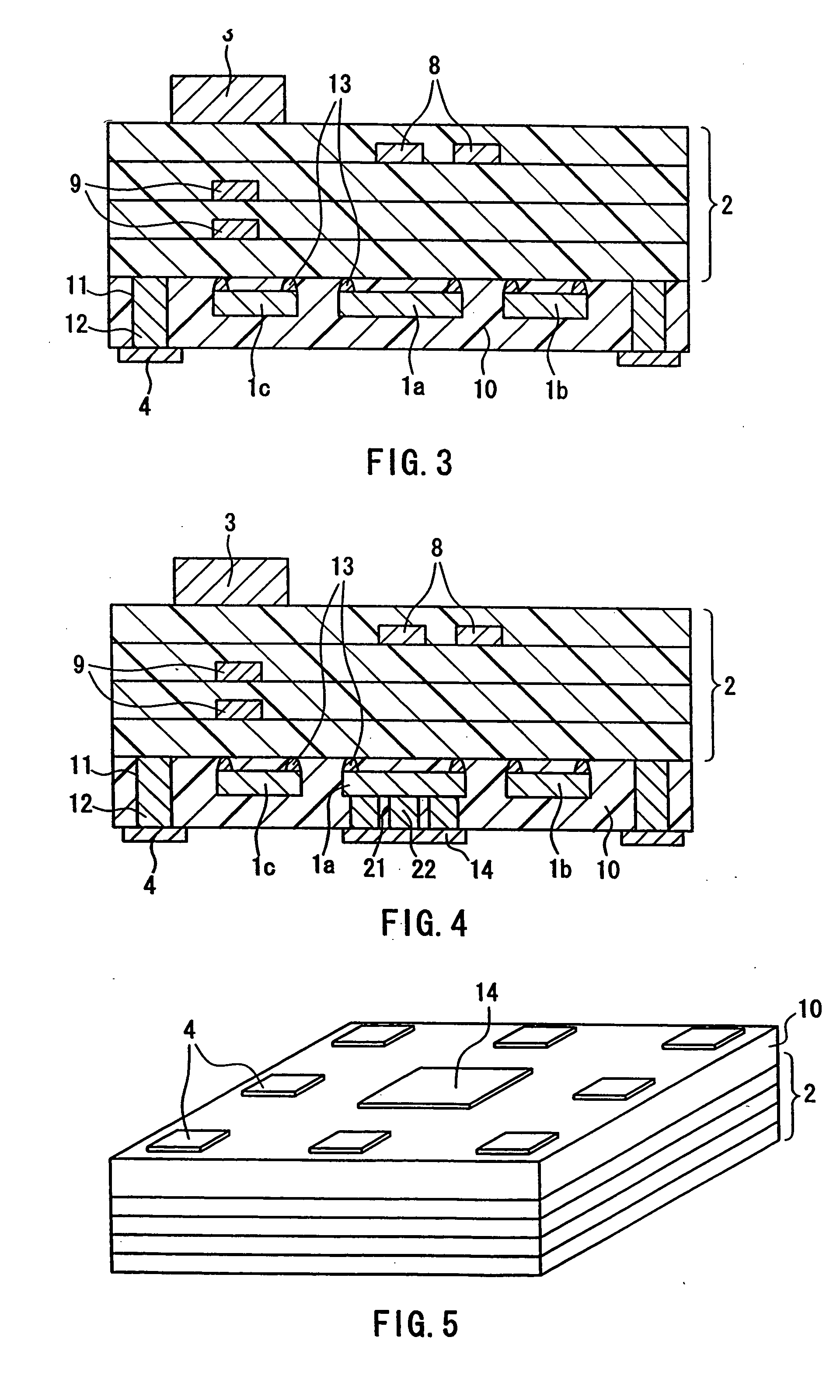
[0052] Embodiment 3
[0053] Embodiment 3 of the invention is described in reference to the cross-sectional view of the high-frequency semiconductor device shown in FIG. 4 and the perspective view of the device of FIG. 4 seen from its rear side shown in FIG. 5.
[0054] The device of FIG. 4 differs from that according to Embodiment 2 shown in FIG. 3 in that interlayer connector via holes 21 are formed directly below the gallium-arsenide power semiconductor element 1a, which is a power amplifier, and a heat-release electrode 14 is formed on the bottom surface of the composite resin material layer 10 in alignment with the positions of the interlayer connector via holes 21. As shown in FIG. 5, a plurality of electrodes 4 for connecting to the outside and the heat release electrode 14, which has a larger area than the electrodes 4 for connecting to the outside, are formed on the bottom surface of the composite resin material layer 10. Accordingly, heat can be released effectively from the el...
PUM
 Abstract
Description
Claims
Application Information