Conductive film and method for preparing the same

a technology of conductive film and conductive film, which is applied in the direction of liquid/solution decomposition chemical coating, semiconductor/solid-state device details, superimposed coating process, etc., can solve the problems of small via hole size, inconvenient for realizing high density, and the effect of high density

Inactive Publication Date: 2005-02-24
FUJIFILM CORP +2
View PDF5 Cites 35 Cited by
  • Summary
  • Abstract
  • Description
  • Claims
  • Application Information

AI Technical Summary

Benefits of technology

The effects of the invention will be made clear with reference to the following Examples, but it should not be construed that the invention is limited to these Examples. Incidentally, the term “part” means “part by weight”.
will be made clear with reference to the following Examples, but it should not be construed that the invention is limited to these Examples. Incidentally, the term “part” means “part by weight”.

Problems solved by technology

In order to cope with this, realization of a high density of printed wiring board becomes a big problem.
Further, though the film thickness of not more than 10 μm is demanded, it is the actual situation that it is likely difficult from the standpoints of handling property and operability to provide a copper thin film having such a film thickness by a pressure roll.
In the multilayered printed wiring board, with respect to a conventional technique of insulating layer prepregs partitioning the planar conductive layer, there is generated a technical problem because of its high density.
However, the formation of a via hole by such drilling is difficult in making the size of the via hole small and is not suitable for realizing a high density.
However, according to the method described in JP-A-4-148590, that is, the method of forming irregularities on the surface of the insulating resin layer by a chemical treatment (surface roughing treatment), since the use of potassium permanganate that may possibly adversely affect the environment is essential in forming irregularities on the surface, such a method is not preferable in view of safety or environment.
However, even this disclosed method is not preferable in view of safety or environment because the treating agent to be used is an oxidizing agent or a strong acid.
Further, according to this method, though the particle-containing photosensitive insulating resin layer is formed by coating, in the case where the particle-containing photosensitive insulating resin layer is provided on an insulating substrate in the lamination (thermo-compression bonding) system that is simple in works of the step and less with respect to defects in the formed layer in comparison with printing or coating, since the particles are dispersed in the photosensitive insulating resin, defects such as incorporation of bubbles onto the insulating substance are liable to be caused, resulting in a problem of difficulty from the standpoint of practical use.

Method used


Image

  • Conductive film and method for preparing the same
  • Conductive film and method for preparing the same
  • Conductive film and method for preparing the same

Examples


example 1

[Case 1] Preparation of Conductive Film 10-A:

(1-1) Preparation of Metal Acetylide (Silver Salt of Illustrative Compound (1)):

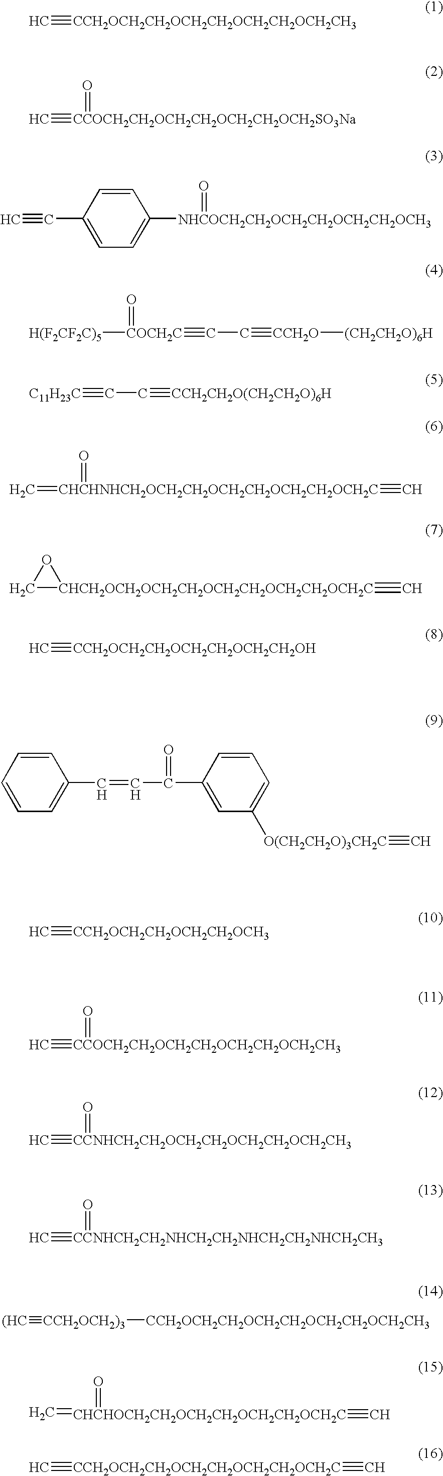
A silver salt of the foregoing Illustrative Compound (1) shown as a specific example of the formula (I) was prepared in the following method.

16.4 g of sodium acetate and 16.7 g of silver nitrate were suspended in 200 mL of distilled water at 40° C. in the light-shielded state. 20.1 g of Illustrative Compound (1) was added dropwise to the suspension, and after stirring for 20 minutes, the mixture was cooled to room temperature. The reaction mixture was neutralized with 7.8 g of sodium hydrogencarbonate, and a supernatant was removed by decantation. Further, 200 mL of distilled water and 400 mL of chloroform were added for extraction. The chloroform layer was dried over anhydrous sodium sulfate, and the chloroform was distilled off in vacuo to obtain 29 g (substantially quantitatively) of a white wax-like solid. It was confirmed from NMR spectrum and IR s...

case 2

[Case 2] Preparation of Conductive Film 20-B:

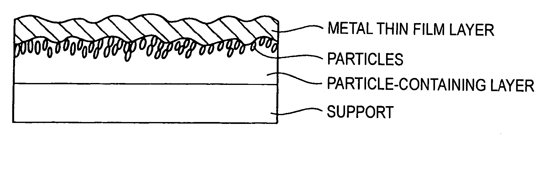
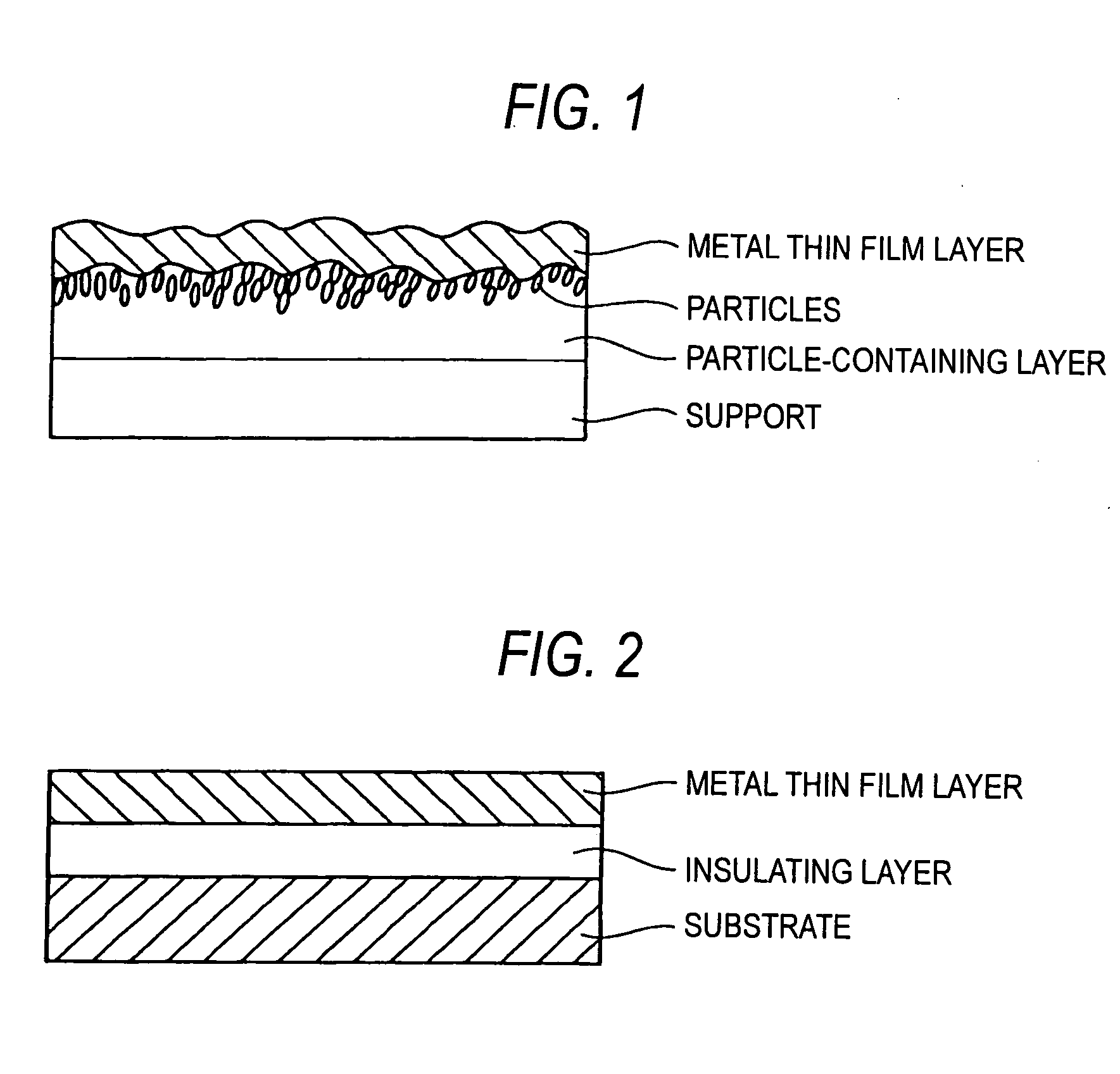
A coating solution a for metallic catalyst layer was prepared in the same operation as in Case 1 and coated on a polyimide resin film (thickness: 50 μm, short-term heat resistant temperature: 420° C.) in a dry film thickness of 0.5 μm using a bar coater. Next, the resulting film was heat treated at 185° C. for 5 minutes to prepare a film in which a metallic silver catalyst layer having fine surface irregularities was formed. This film was dipped in a 1N hydrochloric acid aqueous solution having 500 ppm of palladium chloride dissolved therein for 40 seconds and after washing with water, dried at 100° C. for one hour. The resulting surface had a ten-point mean surface roughness (Rz) of 3.9 μm.

This film was directly subjected to an electrolytic copper plating treatment without subjecting to an electroless copper plating treatment. Similar to Case 1, the electrolytic copper plating liquid had a formulation made of 75 g / L of copper sulfate,...

case 3

[Case 3] Preparation of Conductive Film 10-C:

Preparation of Coating Solution b for Metallic Catalyst Layer:

A coating solution b for metallic catalyst layer having the following formulation was prepared.

Polyvinyl alcohol (10% by weight aqueous32.5 parts by weightsolution: PVA205, manufactured by Kuraray Co.,Ltd.):Polyvinylpyrrolidone (10% by weight aqueous13.8 parts by weightsolution: K905, manufactured by Shin-EtsuChemical Co., Ltd.):Hydroxymethyl cellulose (5% by weight aqueous65.0 parts by weightsolution: TC5E, manufactured by Gokyo TradingCo., Ltd.):Metal acetylide (compound represented by the38.8 parts by weightforegoing structural formula 1 as obtained inCase 1):Finely divided dispersion (the same as in Case59.4 parts by weight2):Surfactant (30% by weight solution: Surflon0.65 parts by weightS131, manufactured by Asahi Glass Co., Ltd.):Ion-exchanged water:40.0 parts by weight

Preparation of Direct Electroless Copper-Plated Film:

The coating solution b for foregoing metall...


PUM

PropertyMeasurementUnit
Temperatureaaaaaaaaaa
Lengthaaaaaaaaaa
Lengthaaaaaaaaaa

Abstract

A conductive film comprising: a support; a particle-containing layer; and a metal thin film layer, in this order, wherein the particle-containing layer contains particles having a mean particle size of from 1 to 10 μm and a heat decomposed material of a metal acetylide and has irregularities derived from a shape of the particles formed on a surface thereof, and the the metal thin film layer contains a metal element.

Description

FIELD OF THE INVENTION The present invention relates to a conductive film and a method of preparing the same. Also, the invention relates to a process of producing a multilayered printed wiring board using a conductive film. BACKGROUND OF THE INVENTION In recent years, the flow of reduction in size and weight and high performance of electronic instruments rapidly advances. For this reason, it is also required to make electronic parts to be used in an electronic instrument small in size. In order to cope with this, realization of a high density of printed wiring board becomes a big problem. The layer structure of a multilayered printed wiring board has a structure in which a planar conductive layer (wiring pattern) and an insulating layer are alternately laminated. Lamination of such a wiring pattern is advantageous in realizing a high density. Hitherto, a 50 μm-thick rolled copper foil has been used because it is cheap and good in handling property. Following the high density of ...

Claims


Application Information

Patent Timeline
IPC IPC(8): C23C18/02B32B15/08C23C18/18C23C28/00C25D5/54H05K3/00H05K3/10H05K3/18H05K3/38
CPCC25D5/54H05K3/105H05K3/181H05K3/38H05K2201/0347Y10T428/25H05K2203/121C23C18/08C23C18/165C23C18/42H05K2203/1105C25D5/56
Inventor KAWATA, KENKOSHIKA, AKIHIKO
Owner FUJIFILM CORP
Why Eureka
Try Eureka