
Laser irradiation method and laser irradiation apparatus, and method for fabricating semiconductor device

Inactive Publication Date: 2005-03-03
SEMICON ENERGY LAB CO LTD
View PDF11 Cites 0 Cited by
  • Summary
  • Abstract
  • Description
  • Claims
  • Application Information

AI Technical Summary

Benefits of technology

The present invention intends to provide a method for, with a CW laser, illuminating a laser light with high production efficiency and a laser irradiation apparatus for carrying out the irradiation of the laser light. In addition, the present invention also intends to provide a method for fabricating a semiconductor device by use of a semiconductor film obtained by carrying out the laser irradiation like this.
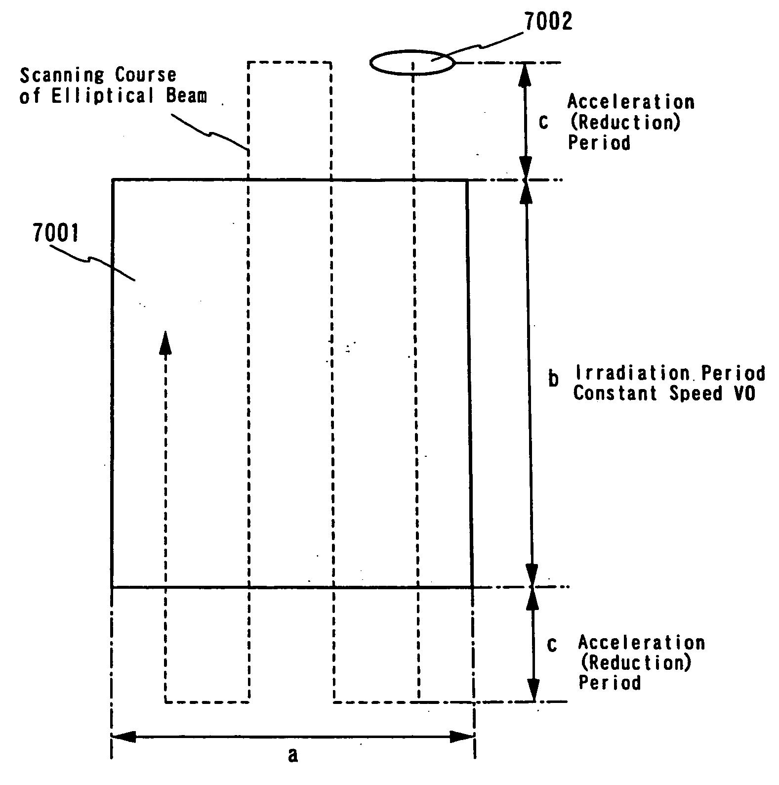
When an entire surface of a semiconductor film formed on a rectangular substrate is laser-annealed according to the present invention, it is obvious that when the elliptical beam is scanned along a longer side of a rectangular substrate the laser annealing can be most efficiently performed. At this time, a major axis of the elliptical beam is arranged so as to be in parallel with a shorter side of the substrate. When thus arranged, the number of times of the acceleration and deceleration of the scanning can be made the least. Accordingly, in Equation 2), it is assumed that a denotes a shorter side of a rectangle and b denotes a longer side thereof. However, since the crystal grain develops in a scanning direction of the laser beam, when in a rectangular substrate a semiconductor element in which grains elongated in the shorter side direction is necessary, there is no problem when a and b may replace each other.
FIGS. 10A through 10C show relationship between the time period necessary for the laser annealing and the scanning speed of the semiconductor film. When the laser annealing is carried out at the V that is substantially one half to twice the scanning speed V calculated from the Equation 6), that is, in the range surrounded by solid lines in FIGS. 10A through 10C, the laser annealing can be efficiently carried out in a time that is substantially 1.3 times or less the time necessary for the shortest laser annealing. Accordingly, the laser annealing need only be carried out in the range of
Preferably, when the laser annealing is carried out at the V in the range of substantially 90% to 110% of the scanning speed calculated from Equation 6), that is, in the range surrounded by the dashed lines in FIGS. 10A through 10C, the laser annealing can be performed in a time substantially the same as that of the shortest annealing and as efficiently as that. Accordingly, the laser annealing may be carried out in the range of

Problems solved by technology

A quartz is an applicable material of substrate for this crystallization, but the quartz substrate is too expensive in price to be manufactured especially in a large area.
In order to improve the productivity efficiency, manufacturing the substrate in a large area is unavoidable, it is expected that a substrate in which a length of one side exceeds 1 m will be also used in recent years.
If the carriers are trapped in trapping centers, potential at a grain boundary will be increased and become barriers to carriers, it is known that current transporting characteristics of carriers will be degraded caused by this.
However, it is almost impossible to form a channel formation region by using a single crystal semiconductor film while avoiding the influence of a crystal boundary, although crystal characteristics of semiconductor film of channel formation region have a serious effect on the TFT characteristics.
However, in this method, since a CW laser having a wavelength in a region that can be sufficiently absorbed by the semiconductor film is used, only a laser that is very small in its output such as substantially 10 W can be applied.
Accordingly, in view of productivity, it is inferior to technology that uses an excimer laser.

Method used


Image

  • Laser irradiation method and laser irradiation apparatus, and method for fabricating semiconductor device
  • Laser irradiation method and laser irradiation apparatus, and method for fabricating semiconductor device
  • Laser irradiation method and laser irradiation apparatus, and method for fabricating semiconductor device

Examples


embodiment 1

[Embodiment 1]

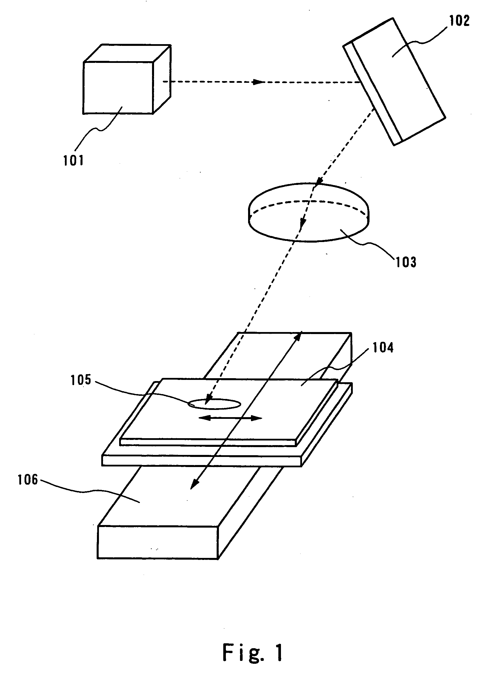
In the present embodiment, in order to compare with the example explained in the implementation mode of the present invention, a case where the scanning speed is set at 50 cm / s will be explained with reference to FIG. 8. A laser oscillator 801 is a CW type 10 W YVO4 laser. A nonlinear optical element is incorporated in a resonator, and second harmonics are emitted therefrom.

A laser beam emitted in a horizontal direction from the laser oscillator 801 is deflected by a mirror 802 into a vertical direction. Thereafter, the laser beam is converged into one direction with a cylindrical lens 803 having a focal length of 150 mm. Furthermore, with a cylindrical lens 804 disposed 100 mm behind the cylindrical lens 803 and having a focal length of 20 mm, the laser beam is converged in a direction that is perpendicular to the one direction and perpendicular to a direction into which the laser beam proceeds. A surface being illuminated 805 where a semiconductor film is disposed...

embodiment 2

[Embodiment 2]

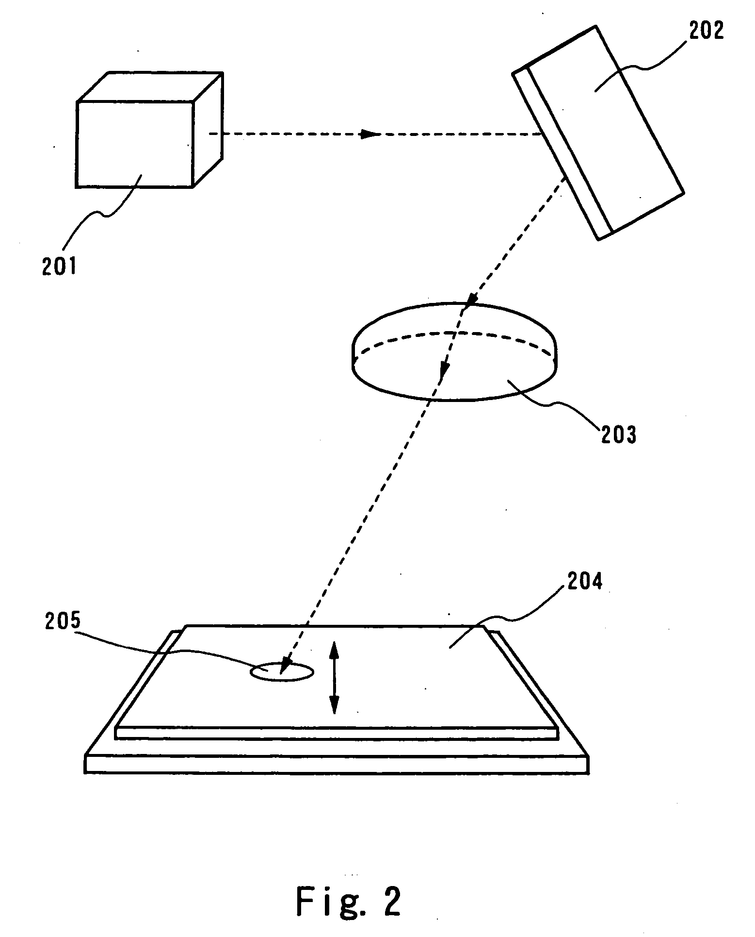
In the present embodiment, in order to compare with the aforementioned example, an example where the scanning speed is set at 500 cm / s will be explained with reference to FIG. 9. A laser oscillator 901 is a continuous wave type 10 W YVO4 laser. A non-linear optical element is incorporated in a resonator, and second harmonics are emitted therefrom.

A laser beam emitted in a horizontal direction from the laser oscillator 901 is deflected by a mirror 902 into a vertical direction. Thereafter, the laser beam is converged into one direction with a cylindrical lens 903 having a focal length of 160 mm. Furthermore, the laser beam is converged with a cylindrical lens 904 disposed 140 mm behind the cylindrical lens 903 and having a focal length of 20 mm into a direction perpendicular to the one direction and perpendicular to a direction into which the laser beam proceeds. The surface being illuminated 905 where the semiconductor film is disposed is disposed at the focal point...

embodiment 3

[Embodiment 3]

In Embodiment 3, an example of the crystallization of the semiconductor film performed by using the optical system of the present invention will be described with reference to FIG. 20.

First of all, a glass substrate made of glasses such as barium borosilicate glass and aluminum borosilicate glass, a substrate which has an insulating film on the surface such as a quartz substrate, a silicon substrate, a metal substrate or stainless substrate, can be used as a substrate 20. The substrate 20 may be a plastic substrate having a heat resistance sufficient to against the processing temperature in this embodiment.

Next, a base film 21 made of an insulating film such as silicon oxide film, silicon nitride film, and a silicon oxynitride film is formed on the substrate 20. In this embodiment, a single layer structure is used for the base film 21. However, a structure may be used where a two or more layers film are stacked. In this embodiment, a silicon oxynitride film (compo...


PUM


Abstract

When a laser beam is radiated on a semiconductor film under appropriate conditions, the semiconductor film can be crystallized into single crystal-like grains connected in a scanning direction of the laser beam (laser annealing). The most efficient laser annealing condition is studied. When a length of one side of a rectangular substrate on which a semiconductor film is formed is b, a scanning speed is V, and acceleration necessary to attain the scanning speed V of the laser beam relative to the substrate is g, and when V=(gb / 5.477)1 / 2 is satisfied, a time necessary for the laser annealing is made shortest. The acceleration g is made constant, however, when it is a function of time, a time-averaged value thereof can be used in place of the constant.

Description

BACKGROUND OF THE INVENTION 1. Field of the Invention The present invention relates to a laser beam irradiation method and a laser irradiation apparatus for using the method (apparatus including a laser and an optical system for guiding laser beam emitted from the laser to an object to be illuminated). In addition, the present invention relates to a method of manufacturing a semiconductor device, which includes a laser beam irradiation step. Note that a semiconductor device described here includes an electro-optical device such as a liquid crystal display device or a light-emitting device, and an electronic device that includes the electro-optical device as a part. 2. Description of the Related Art In recent years, an extensive study has been made on a technique in which an amorphous semiconductor film formed on an insulating substrate made of glass or the like is crystallized so that a semiconductor film having crystal structure (hereafter referred to as crystalline semiconduct...

Claims


Application Information

Patent Timeline
IPC IPC(8): H01L21/20H01L21/268
CPCH01L21/2026Y10S117/904H01L21/268H01L21/02683H01L21/02422H01L21/02488H01L21/0242H01L21/02672H01L21/02425H01L21/02686H01L21/02678H01L21/02532H01L21/02595H01L21/02381H01L21/02691
Inventor YAMAZAKI, SHUNPEITANAKA, KOICHIRO
Owner SEMICON ENERGY LAB CO LTD
Learn More