Epitaxial mode-confined vertical cavity surface emitting laser (VCSEL) and method of manufacturing same

a vertical cavity surface and laser technology, applied in semiconductor lasers, laser details, optical resonator shape and construction, etc., can solve the problems of lateral definition of both, high device performance damage, optical loss, etc., and achieve low threshold current, high efficiency, and high speed

Inactive Publication Date: 2005-03-24
DEPPE DENNIS G
View PDF15 Cites 52 Cited by
  • Summary
  • Abstract
  • Description
  • Claims
  • Application Information

AI Technical Summary

Benefits of technology

The disclosed embodiments of a VCSEL include an intracavity epitaxial layer configured to include a shallow mesa that alters the optical mode of the vertical cavity to laterally confine the optical mode in an otherwise planar epitaxial cavity. Therefore while the cavity may be nearly planar with respect to its crystal surfaces, the mesa leads to the creation of at least two distinct cavity types. Although mirrors of the VCSEL may be augmented by additional dielectric or metal layers, in some embodiments the mesa and mirror layers that cover the mesa are epitaxial. The VCSEL has optical confinement and current confinement within nearly the same active area and thus can operate with low threshold current, high efficiency, or high speed. The use of epitaxial DBRs eliminates strain in the semiconductor device, ensuring high reliability. The epitaxial DBRs also provide high reflectivity and low optical loss.
Some embodiments of the VCSEL provide a mode confining region (i.e., mesa) that is defined using a lithography process. This lithographic process eliminates external process variations such as material composition or thickness variation from influencing the mode confining region's size. The result is a highly uniform structure across a semiconductor wafer and from wafer to wafer. Another advantage of the VCSEL is that the optical confinement and current confinement regions are self-aligned because the same manufacturing steps are used to form both. In some embodiments, the optical mode area is substantially different from the current injection area of the active material, but the current confinement area and the optical mode area are concentric or nearly concentric.

Problems solved by technology

A historical problem has been the lateral definition of both the optical mode and the electrical current injection region.
However, laterally confining the optical mode can also introduce optical loss, which is highly detrimental to the device performance.
However, this type of device suffers increasing optical loss due to optical scattering at the surfaces of the pillar as the pillar diameter is reduced.
It is also prone to surface degradation over time which causes poor reliability.
Some proton implanted VCSELs have high device reliability and are based on a simple fabrication process, but the optical loss is high due to the lack of an optical guide to confine the lasing mode.
Thus, these devices suffer from a relatively high threshold current and low modulation speed, and unstable lasing modes.
However, the need to form the oxide aperture by converting AlxGa1-xAs to a native oxide is plagued with several manufacturing problems.
In addition, the native oxide has a different thermal expansion coefficient from that of the surrounding semiconductor material of the VCSEL, and the strain that this difference induces inside the device can cause a substantial reliability problem and early device failure.
Another limitation is that the native oxide process has thus far proven effective only for AlxGa1-xAs, while other materials are desirable for VCSELs that operate at wavelengths that cannot be produced using GaAs / AlGaAs materials.
As discussed in detail later, these scattering losses can come from either the optical cavity partially covered with an electrode or the poor mode matching that comes from using a recessed region in an attempt to confine the optical mode.
This optical loss can increase the VCSEL's threshold and decreases it efficiency.
However, these researchers also do not consider how the optical mode is scattered by the recessed region, and temperature changes across the device can lead to mode instability due to its compensation of diffraction loss caused by the recessed regions.
This VCSEL device has the drawback that the dielectric mirror material is different than the semiconductor used in the VCSEL, and can therefore add mechanical stress to the VCSEL and reduce its reliability.
This VCSEL, however, can also suffer mechanical strain due to mismatch of its materials, and therefore reduced reliability.
These approaches that are fully planar and all epitaxial generally do not provide the optical mode confinement to produce low threshold or high efficiency VCSELs needed for high speed modulation.

Method used


Image

  • Epitaxial mode-confined vertical cavity surface emitting laser (VCSEL) and method of manufacturing same
  • Epitaxial mode-confined vertical cavity surface emitting laser (VCSEL) and method of manufacturing same
  • Epitaxial mode-confined vertical cavity surface emitting laser (VCSEL) and method of manufacturing same

Examples


example 1

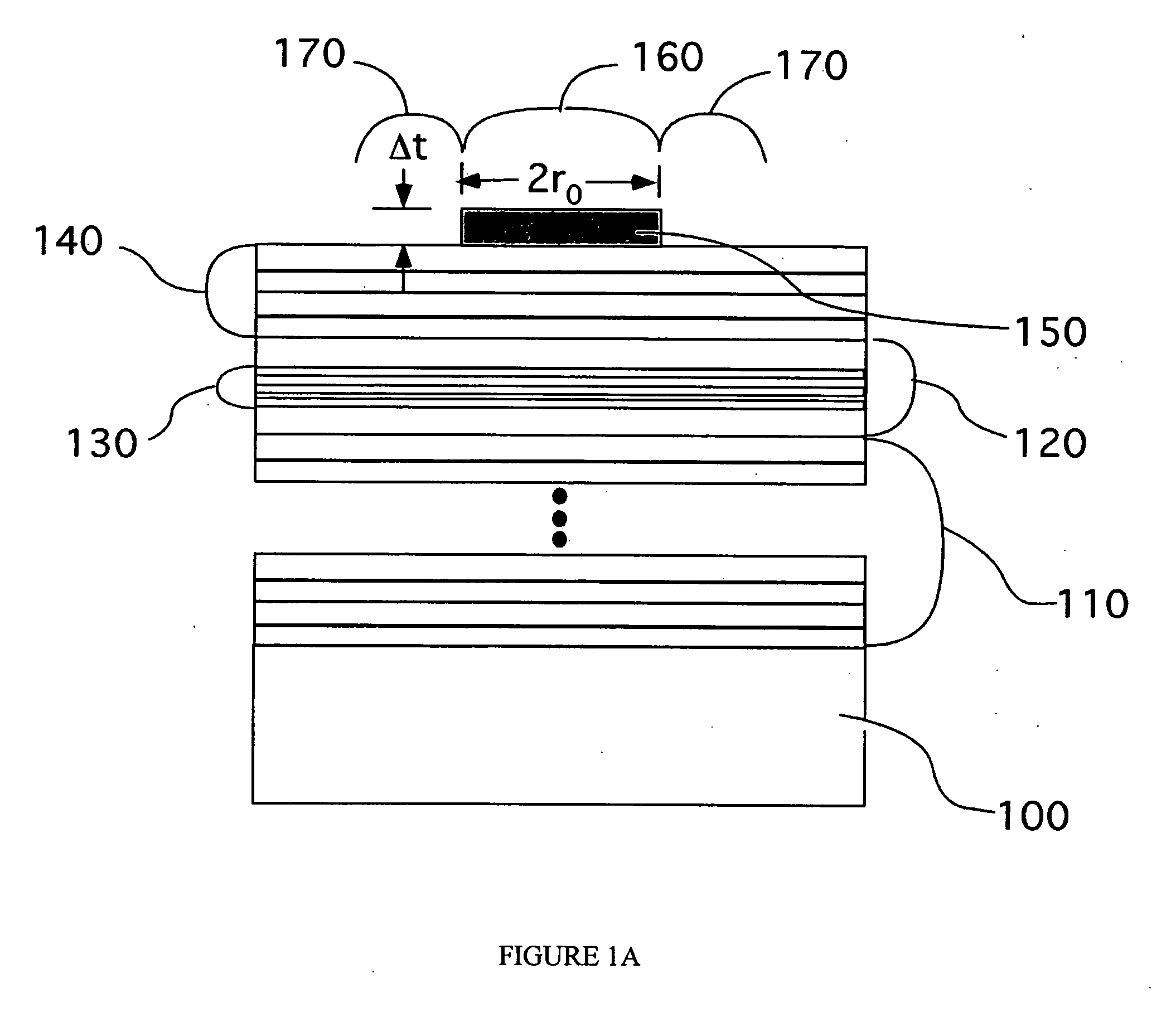
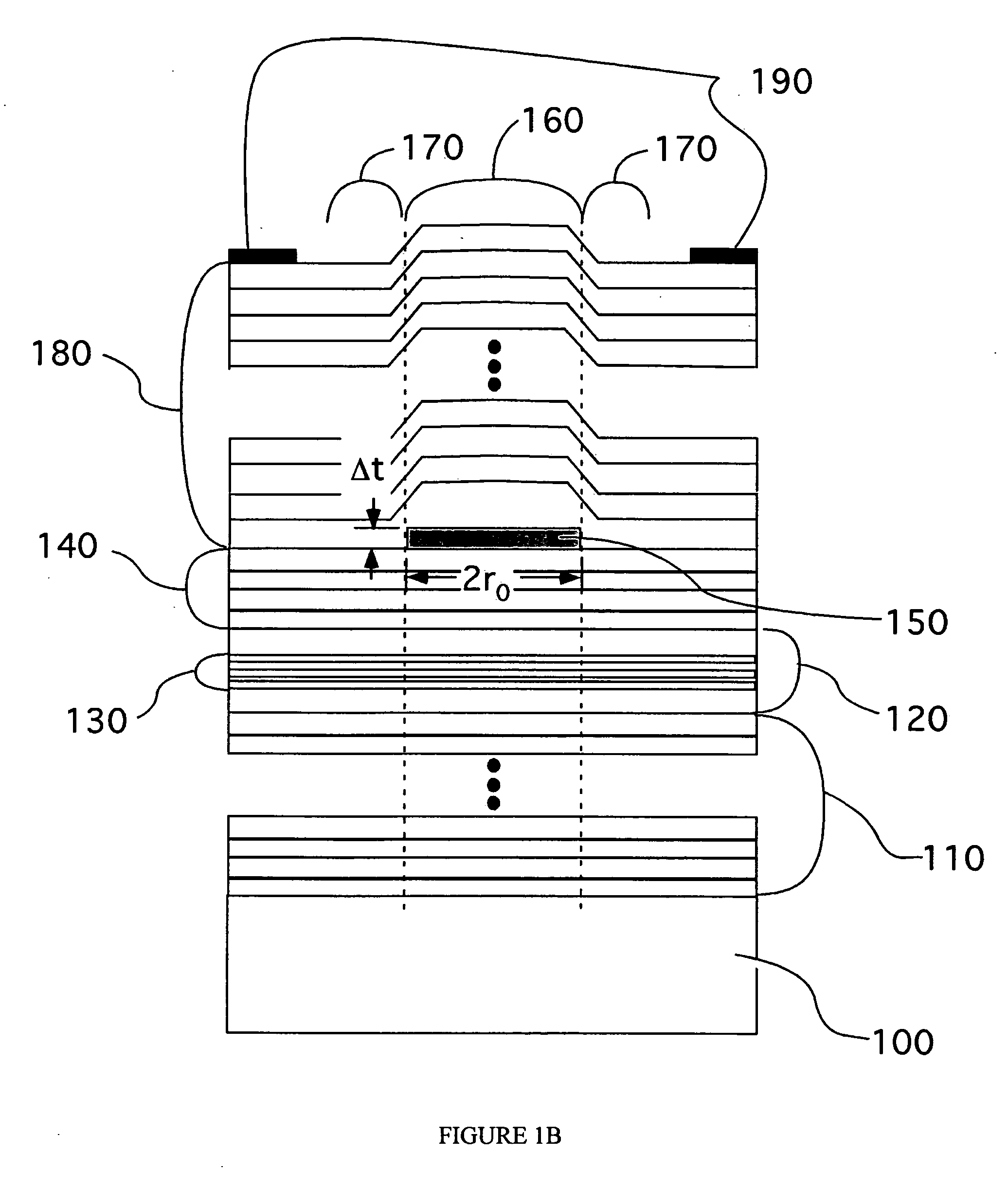
Reference is first made to FIG. 1A. FIG. 1A shows a schematic illustration of the heterostructure of a partial semiconductor VCSEL cavity. To form the partial cavity an epitaxial growth is performed on a substrate, layer 100, which may also contain various buffer layers used to prepare the crystal for growth of a lower DBR mirror layers 110. The lower DBR typically consists of semiconducting layers nominally lattice-matched to the substrate, but in some cases, for example for nitride semiconductors, the substrate may be sapphire or SiC. For AlGaAs VCSELs the substrate is generally GaAs. The lower DBR typically consists of alternating layers of semiconductors, for example AlxGa1-xAs / AlyGa1-yAs, with alternating refractive indices in the layers to cause a constructive interference in the reflections of the DBR and yield high reflectivity at the desired wavelength. On this lower DBR layer 110 is grown an active region 120 consisting of a spacer layer and active layers 130 made of eith...

example 2

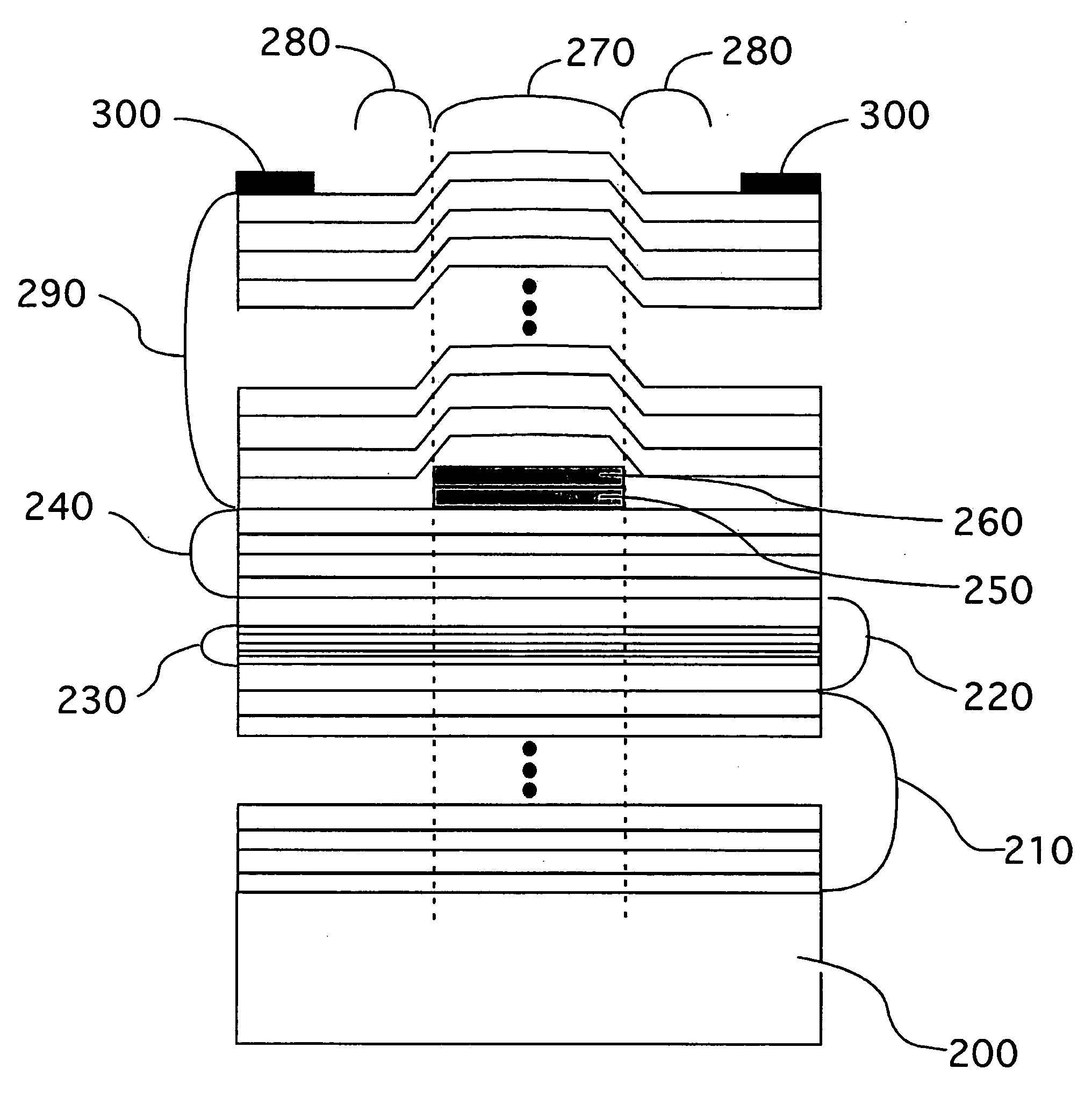
FIG. 2 shows an embodiment used to confine electrical current to the same epitaxial mesa that confines the optical mode based on a tunnel junction. Layer 200 is a substrate receiving epitaxial crystal growth, on which may also be initially deposited buffer layers for surface smoothing and preparation. Layer 210 is a lower DBR mirror with at least the upper portion closest to layers 220 containing impurity doping to make it electrically conductive. Typically, for AlGaAs VCSELs it is desirable to dope these upper layers n-type with Si, Se, or other n-type impurities. The active layer 220, and a portion of the upper mirror 240 and the mesa forming layers 250 and 260 can be grown in the same growth step. Assuming the upper part of the lower mirror, layers 210 are doped n-type, the upper mirror layers 240 are doped p-type using impurities such as C, Be, Zn, Mg, or others, to form a p-n junction for electron and hole injection into the active layers 220. These electrons and holes are then...

example 3

Referring to FIG. 6, a lower semiconductor DBR consisting of layers 310 is grown on substrate 300, that may include additional buffer layers, followed by an active region 320 containing active layers 330 that confine electron and hole charge carriers. The upper DBR includes layers 340, with a pair number that may vary from zero or greater, and a mesa layer 350. Following epitaxial growth impurities are introduced into the upper cavity region layers 340 to form the crystal regions 390, using either diffusion or implantation, while masking the mesa layer 350 and the crystal region beneath it from the impurities. In this embodiment at least the upper region of the lower DBR layers 310 adjacent to the active region 320 are doped with n-type impurities grown into the crystal, while the upper layers 340 and mesa forming layer 350 are doped p-type. The selective introduction of impurities outside the mesa layer 350 can be performed using diffusion or implantation with the same masking mat...


PUM


Abstract

A Vertical Cavity Surface Emitting Laser (VCSEL) includes an intracavity epitaxial layer configured to include a shallow mesa that alters the optical mode of the vertical cavity to laterally confine the optical mode in an otherwise planar epitaxial cavity. The VCSEL has optical confinement and current confinement within nearly the same active area and thus can operate with low threshold current, high efficiency, or high speed. In some embodiments, a mode confining region (i.e., mesa) is defined using a lithography process. This lithographic process eliminates external process variations such as material composition or thickness variation from influencing the mode confining region's size. The result is a highly uniform structure across a semiconductor wafer and from wafer to wafer. In some embodiments, the optical confinement and current confinement regions are self-aligned because the same manufacturing steps are used to form both. In other embodiments, the optical mode area is substantially different from the current injection area of the active material, but the current confinement area and the optical mode area are concentric or nearly concentric.

Description

TECHNICAL FIELD This invention relates generally to solid-state optoelectronics devices, and more particularly relates to semiconductor vertical cavity surface emitting lasers (VCSELs). BACKGROUND A vertical cavity surface emitting laser (VCSEL) can be formed from epitaxial semiconductor mirrors to create a very compact, low optical loss, all-semiconductor microcavity. The VCSEL has become an important laser device, because it can operate efficiently at low power levels with good beam characteristics, and is relatively easy to manufacture. VCSELs have applications in fiber optic transceivers, bar code scanners, compact disk storage, displays, solid state lighting, and others. VCSELs typically include a GaAs substrate on which AlxG1-xAs / AlyGa1-yAs distributed Bragg reflecting (DBR) mirrors and active materials are grown using single crystal epitaxy. Other semiconductor or non-semiconductor substrates, such as InP or sapphire, can be used with different active materials to create VC...

Claims


Application Information

Patent Timeline
Patent Type & Authority Applications(United States)
IPC IPC(8): H01S5/183
CPCH01S5/18308H01S5/18327H01S2301/18H01S5/18388H01S5/3095H01S5/1833
Inventor DEPPE, DENNIS G.
Owner DEPPE DENNIS G
Why Eureka
Try Eureka