System and process for producing nanowire composites and electronic substrates therefrom

Active Publication Date: 2005-03-24
ONED MATERIAL INC
View PDF66 Cites 238 Cited by
  • Summary
  • Abstract
  • Description
  • Claims
  • Application Information

AI Technical Summary

Benefits of technology

[0019] In another aspect, the present invention relates to a process for producing a high capacitance capacitor, and a capacitor produced by the process. The process comprises providing a free-standing nanowire-material composite, depositing a metal on both surfaces of the composite film, depositing an insulator on a metal surface to form a capacitor film, and assembling a capacitor. The assembling step comprises optional further processing steps including, but not limited to attaching leads to the metal surfaces, rolling the capacitor film and sealing the film in a canister. The nanowires are optionally oriented in the nanowire-materi

Problems solved by technology

However, amorphous silicon and organic semiconductors have performance limitations.
Furthermore, they require relatively expensive processes, such as laser induced annealing, to improve their performance.
While nanowires show promise as high mobility electrical carriers, their use in devices is currently limited by difficulties that arise in harvestin

Method used


Image

  • System and process for producing nanowire composites and electronic substrates therefrom
  • System and process for producing nanowire composites and electronic substrates therefrom
  • System and process for producing nanowire composites and electronic substrates therefrom

Examples


composite embodiments

NANOWIRE COMPOSITE EMBODIMENTS

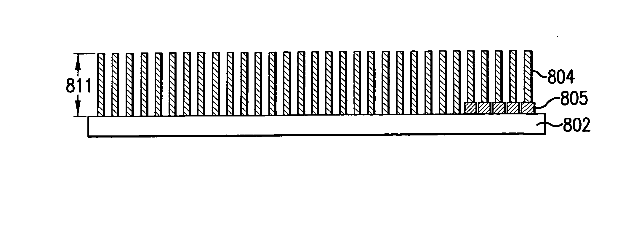
[0111] In another aspect, the invention relates to a system and process for producing a nanowire-material composite. For example, FIG. 5 shows a flowchart 500 showing example steps for producing a nanowire-material composite, according to an embodiment of the present invention. FIGS. 6A-6C show example implementations of the steps of FIG. 5. Flowchart 500 begins with step 502. In step 502, a substrate having nanowires attached to a portion of at least one surface is provided. In step 504, a material is deposited over the portion to form the nanowire-material composite. Flowchart 500 optionally further includes step 506. In step 506, the nanowire-material composite is separated from the substrate to form a freestanding nanowire-material composite.

[0112]FIG. 6A shows an example implementation of step 502. Referring to FIG. 6A, a substrate 602 is provided having nanowires 606 attached to a portion 604. Portion 604 can be all or less than an entire area of...

example 1

Preparation of Nanowire Composite with Nanowires Oriented Perpendicular to the Sheet Surface

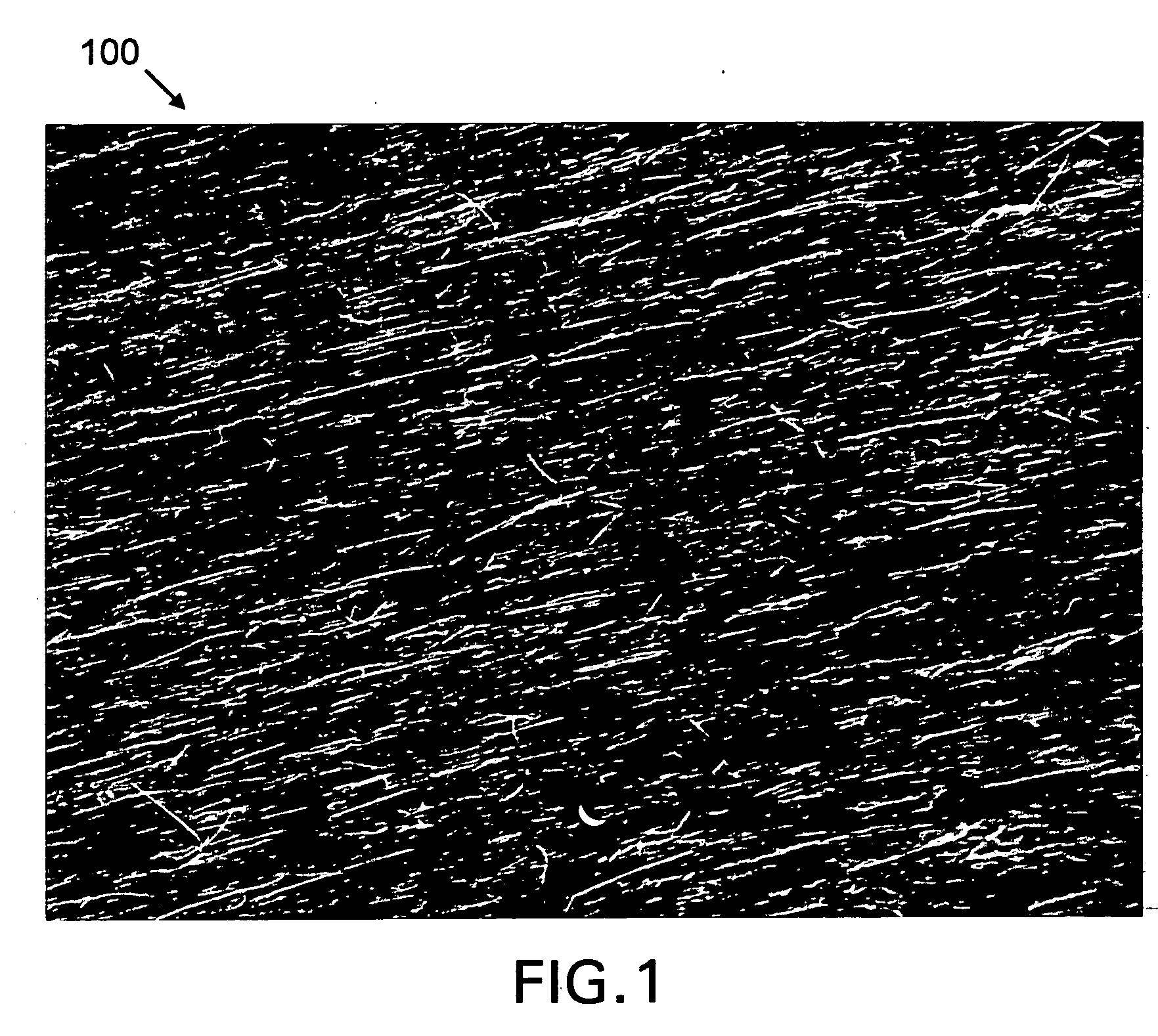
[0183] About 1.0 g of liquid polyethylene glycol diacrylate comprising about 10 mg of the photo initiator 2,2-dimethoxy-2-phenylacetophenone was placed in a glass vial. A silicon substrate, measuring about 1×3 cm was coated with 40 nm in diameter silicon nanowires. The nanowires were oriented substantially perpendicular to the surface of the substrate. The substrate was placed in the glass vial, with about 3 mm of one end of the substrate immersed in the liquid mixture. After about 15 minutes, the nanowires had wicked the liquid up to fill the spaces between them. The substrate was removed from the vial and placed under a UV lamp for about 15 min to polymerize the liquid. A nanocomposite coated substrate was thereby obtained, in which the nanowires were “frozen” at their original growth orientation.

[0184]FIG. 31 is a Scanning Electron Microscope (SEM) image of nanowires oriented perpendicul...

example 2

Preparation of Nanowire Composite with Nanowires Oriented Perpendicular to the Sheet Surface

[0185] About 0.5 g poly(vinylidenefluoride) (PVDF) polymer was contacted with about 10 g of acetone. After a clear solution formed, about 11.6 mg of 40 nm Si nanowires was dispersed into the solution by sonication. About 5 g of the dispersion was transferred to a flat bottom glass dish with an inner diameter of about 35 mm. The dish was placed between a pair of electrodes and a DC field (about 3000 V / cm, with the negative (−) electrode applied to the top and positive (+) electrode applied to the bottom) was applied and the solvent was evaporated under the field.


PUM


Abstract

The present invention relates to a system and process for producing a nanowire-material composite. A substrate having nanowires attached to a portion of at least one surface is provided. A material is deposited over the portion to form the nanowire-material composite. The process further optionally comprises separating the nanowire-material composite from the substrate to form a freestanding nanowire-material composite. The freestanding nanowire material composite is optionally further processed into a electronic substrate. A variety of electronic substrates can be produced using the methods described herein. For example, a multi-color light-emitting diode can be produced from multiple, stacked layers of nanowire-material composites, each composite layer emitting light at a different wavelength.

Description

BACKGROUND OF THE INVENTION [0001] 1. Field of the Invention [0002] The present invention relates to semiconductor devices, and more particularly, to the preparation of active elements for use in semiconductor devices. [0003] 2. Related Art [0004] An interest exists in industry in developing low cost electronics, and in particular, in developing low cost, large area electronic devices. Availability of such large area electronic devices could revolutionize a variety of technology areas, ranging from civil to military applications. Example applications for such devices include driving circuitry for active matrix liquid crystal displays (LCDs) and other types of matrix displays, smart libraries, credit cards, radio-frequency identification tags for smart price and inventory tags, security screening / surveillance or highway traffic monitoring systems, large area sensor arrays, and the like. [0005] Current approaches involve using amorphous silicon or organic semiconductors as the base ma...

Claims


Application Information

Patent Timeline
IPC IPC(8): D02G3/00H01L21/336H01L21/44H01L29/06H01L29/423H01L29/786H01L33/06H01L33/24H01L51/00H01L51/05
CPCB82Y10/00Y10T428/2913H01L29/0673H01L29/0676H01L29/068H01L29/42384H01L29/66742H01L29/78681H01L29/78696H01L33/06H01L33/24H01L51/0048H01L51/0545H01L29/0665H01L2924/0002H01L2924/00H10K85/221H10K10/466
Inventor BURETEA, MIHAICHEN, JIANCHOW, CALVINNIU, CHUNMINGPAN, YAOLINGPARCE, J. WALLACEROMANO, LINDA T.STUMBO, DAVID
Owner ONED MATERIAL INC
Why Eureka
Try Eureka