Copper bath for electroplating fine circuitry on semiconductor chips

a technology of fine circuitry and copper bath, which is applied in the manufacture of printed circuits, basic electric elements, electric apparatus, etc., can solve the problems of difficult to achieve close control, complex additive system, and inability to accept damascene copper deposits, so as to prevent runaway copper electrodeposition, improve the deposit properties, and avoid interference from breakdown products

Inactive Publication Date: 2005-03-31
INNOVATIVE TECH LICENSING
View PDF4 Cites 25 Cited by
  • Summary
  • Abstract
  • Description
  • Claims
  • Application Information

AI Technical Summary

Benefits of technology

[0020] This invention provides an electroplating bath based on a strongly complexing anion and an accelerating additive for electrodepositing copper circuitry in Damascene trenches and vias on semiconductor chips. This bath avoids the disadvantages of the acid copper sulfate baths employed for Damascene plating in the prior art. Use of a strongly complexing anion (pyrophosphate or cyanide, for example) to suppress runaway copper electrodeposition and improve the deposit properties eliminates the need for the polymeric suppressor additive used in acid copper sulfate baths, and avoids interference from breakdown products thereof. Bottom-up filling of Damascene features is provided by a single accelerating additive species. This additive is present at low concentrations and is not rapidly consumed in the copper electrodeposition process so that organic breakdown products are minimal. The low accelerating additive concentration used and the inherently good throwing power of strongly complexed baths tend to provide a uniform “overburden” layer, which is more easily removed by chemical mechanical planarization (CMP) and obviates the need for the “leveler” additive employed in acid copper sulfate baths. The strongly complexing anion is present in high concentration and is not rapidly consumed in the electrodeposition process, which facilitates control of the plating system.
[0021] In addition, the strongly complexed copper electroplating baths of the present invention provide relatively fine-grained deposits that have stable properties, whereas acid copper sulfate deposits are generally large-grained and must be annealed to stabilize key deposit properties (e.g., hardness and electrical conductivity). The fine-grained deposits from the strongly-complexed bath of the invention also tend to be harder and more resistant...

Problems solved by technology

An imbalance in the additive system typically results in unacceptable voids or defect lines in the Damascene copper deposit, formed as the copper deposits on opposing sidewalls of the feature grow together (in the absence of bottom-up filling).
A major disadvantage of the acid copper sulfate system for Damascene plating is the complicated additive system, whose components must be closely controlled to obtain acceptable deposits.
Close control is difficult to attain since the various additive species are generally present at very low concentrations and exert synergistic effects.
Plating bath suppliers typically provide organic additives in the form of solutions that may contain additives of more than one type (as well as inorganic species), which exacerbates the difficulty of controlling the additive system.
Furthermore, additive breakdown products tend to accumulate in the plating bath and interfere with functioning of the additive system.
Additive breakdown products are typically removed by bleeding off part of the plating bath and replacing it with fresh plating solution (bleed-and-feed), which is costly and environmentally undesirable.
Another disadvantage of the acid copper sulfate system for Damascene plating is that key properties of the deposit (grain size, hardness and electrical conductivity) undergo slow changes at ambient temperatures.
), which adds an extra processing step and increases costs.
Still another disadvantage of the acid copper sulfate system for Damascene plating is that the copper deposit tends to be relatively soft (large-grained).
During CMP processing, soft copper tends to be removed faster than the surrounding dielectric material and, especially for wide trenches and bond pads, may “dish” and lose the planarity needed to facilitate bonding and minimize circuit electrical resistance.
Still another disadvantage o...

Method used


Image

  • Copper bath for electroplating fine circuitry on semiconductor chips
  • Copper bath for electroplating fine circuitry on semiconductor chips
  • Copper bath for electroplating fine circuitry on semiconductor chips

Examples


example 1

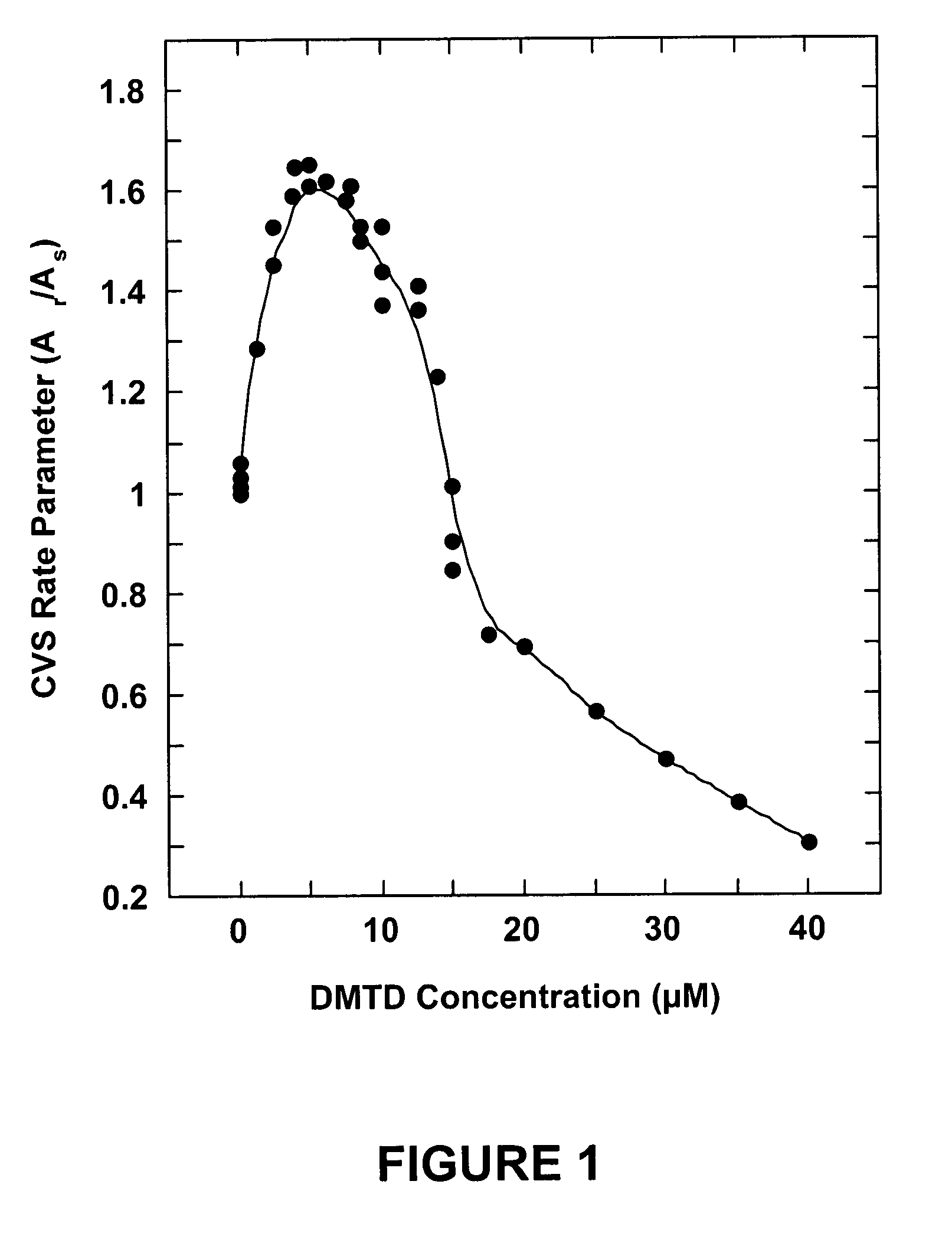
[0058] Coupons were plated from copper pyrophosphate solutions (55° C.) containing 0.0, 0.33, 0.67, 1.0, 1.3, 1.7, 2.0, 2.3, 3.3, 5.0 or 8.3 μM of the DMTD additive (without surfactant added). Good bottom-up filling of the smallest features (0.13 μm vias) was attained with the 2.0 μM solution, as indicated by the micrograph in FIG. 6. Good bottom-up filling of all of the larger features (0.20, 0.33 and 0.38 μm wide) was attained with the 1.3, 1.7 and 2.0 μM solutions. Incomplete filling was observed for all features with all of the other solutions, except that good bottom-up filling was observed for the two larger features (0.33 and 0.37 μm wide) with the 3.3 μM solution. These data show that the DMTD monomer additive of the present invention provides good bottom-up filling of Damascene features as fine as 0.13 μm wide (5.4:1 aspect ratio). The optimum DMTD concentration was about 2 μM for the conditions used but would be expected to depend on the plating parameters, such as current...

example 2

[0059] Coupons were plated from copper pyrophosphate solutions (55° C.) containing 0.50 g / L Triton®-X surfactant and 0.0, 0.33, 0.67, 1.0, 1.3, 1.7, 2.0, or 5.7 μM of the DMTD additive. As was the case without surfactant added, a DMTD concentration of about 2 μM provided good bottom up filling of even the smallest Damascene features (0.13 μm vias) in the presence of the Triton®-X surfactant.


PUM

PropertyMeasurementUnit
Temperatureaaaaaaaaaa
Molar densityaaaaaaaaaa

Abstract

Bottom-up filling of fine Damascene trenches and vias in semiconductor chips is attained using a copper pyrophosphate electroplating bath with a single accelerating additive species present at low concentration (<5 μM). This bath is much easier to control than the acid copper sulfate bath, which employs a complicated additive system involving a minimum of two organic additives and chloride ion (as well as significant additive breakdown products). Pyrophosphate copper deposits exhibit stable properties without annealing and are typically twice as hard as acid sulfate copper deposits, which facilitates chemical mechanical planarization. The mechanical properties and texture of the fine-grained pyrophosphate copper deposits are also much less substrate dependent, which minimizes the effects of variations and flaws in the barrier and seed layers. Attack of copper seed layers is minimized for the copper pyrophosphate bath, which operates in the pH 8 to 9 range. The resistivity of pyrophosphate and annealed acid sulfate copper deposits are substantially equivalent.

Description

BACKGROUND OF THE INVENTION [0001] 1. Field of the Invention [0002] This invention is concerned with fabrication of copper integrated circuits on semiconductor chips, and in particular with electrodeposition of copper circuitry. [0003] 2. Description of the Related Art [0004] The electronics industry is transitioning from aluminum to copper as the basic metallization for semiconductor integrated circuits (IC's) in order to increase device switching speed and enhance electromigration resistance. The leading technology for fabricating copper circuitry on semiconductor chips is the “Damascene” process (P. C. Andricacos, Electrochem. Soc. Interface, Spring 1999, p.32; U.S. Pat. No. 4,789,648 to Chow et al.; U.S. Pat. No. 5,209,817 to Ahmad et al.). In this process, vias are etched in the chip's dielectric material, which is typically silicon dioxide, although materials with lower dielectric constants are under development. A barrier layer, e.g., titanium nitride (TiN), tantalum nitride ...

Claims


Application Information

Patent Timeline
IPC IPC(8): C25D3/38C25D3/58H01L21/288H01L21/768H05K3/42
CPCC25D3/38C25D3/58H05K3/423H01L21/76877H01L21/2885
Inventor TENCH, D. MORGANWHITE, JOHN T.
Owner INNOVATIVE TECH LICENSING
Why Eureka
Try Eureka