Laser processing of a locally heated target material

a local heating and laser processing technology, applied in the field of laser processing a local heating workpiece, can solve the problems of reducing the energy density of the laser output, the inability to form through-hole vias using cosub>2 /sub>lasers, and the difficulty of forming through-hole vias in copper sheets having a thickness greater than about 5 microns, etc., to achieve the effect of improving the rate of material removal and workpiece throughput, improving process quality, and improving speed speed or efficiency

Inactive Publication Date: 2005-04-28
ELECTRO SCI IND INC
View PDF8 Cites 69 Cited by
  • Summary
  • Abstract
  • Description
  • Claims
  • Application Information

AI Technical Summary

Benefits of technology

[0016] An object of the present invention is, therefore, to provide a method of and a laser system for improving the speed and / or efficiency of (1) laser processing via and / or holes in single and multilayer workpieces and (2) dicing semiconductor wafers such that the rates of material removal and workpiece throughput are increased and process quality is improved.

Problems solved by technology

The diameter of the spot size can be enlarged to have the same diameter as the desired diameter of the via, but this enlargement reduces the energy density of the laser output such that it is less than the ablation threshold of the target material and cannot effect target material removal.
However, a via having a spot area diameter of less than 50 μm cannot be formed using a CO2 laser.
The high degree of reflectivity of the copper at the CO2 wavelength makes forming a through-hole via using a CO2 laser in a copper sheet having a thickness greater than about 5 microns very difficult.
Thus laser processing throughput, such as, for example, via formation on PCB or other electronic packaging devices or hole drilling on metals or other materials, is limited by the laser power intensity available and pulse repetition rate, as well as the speed at which the beam positioner can move the laser output in a spiral, concentric circle, or trepan pattern and between via positions.
However, for the UV DPSS laser and the pulsed CO2 laser, there are practical problems stemming from the amounts by which the laser energy per pulse and the pulse repetition rate can be increased.
Moreover, as laser energy per pulse increases, the risk of damage to the optical components inside and outside the laser resonator increases.
Repairing damage to these optical components is especially time-consuming and expensive.
Additionally, lasers capable of operating at a high laser energy per pulse or a high pulse repetition rate are often prohibitively expensive.
Mechanically sawing wafers having a thickness that is less than about 100 microns results in cracking of the wafer.
However, one disadvantage of laser dicing semiconductor wafers is the formation of debris and slag, both of which could adhere to the wafer and are difficult to remove.
Another disadvantage of laser dicing semiconductor wafers is that the workpiece throughout rate is limited by the power capabilities of the laser.

Method used


Image

  • Laser processing of a locally heated target material
  • Laser processing of a locally heated target material
  • Laser processing of a locally heated target material

Examples


first embodiment

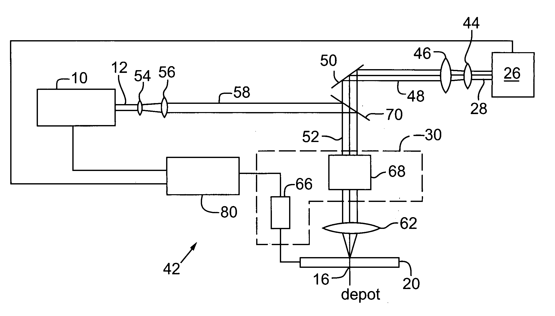
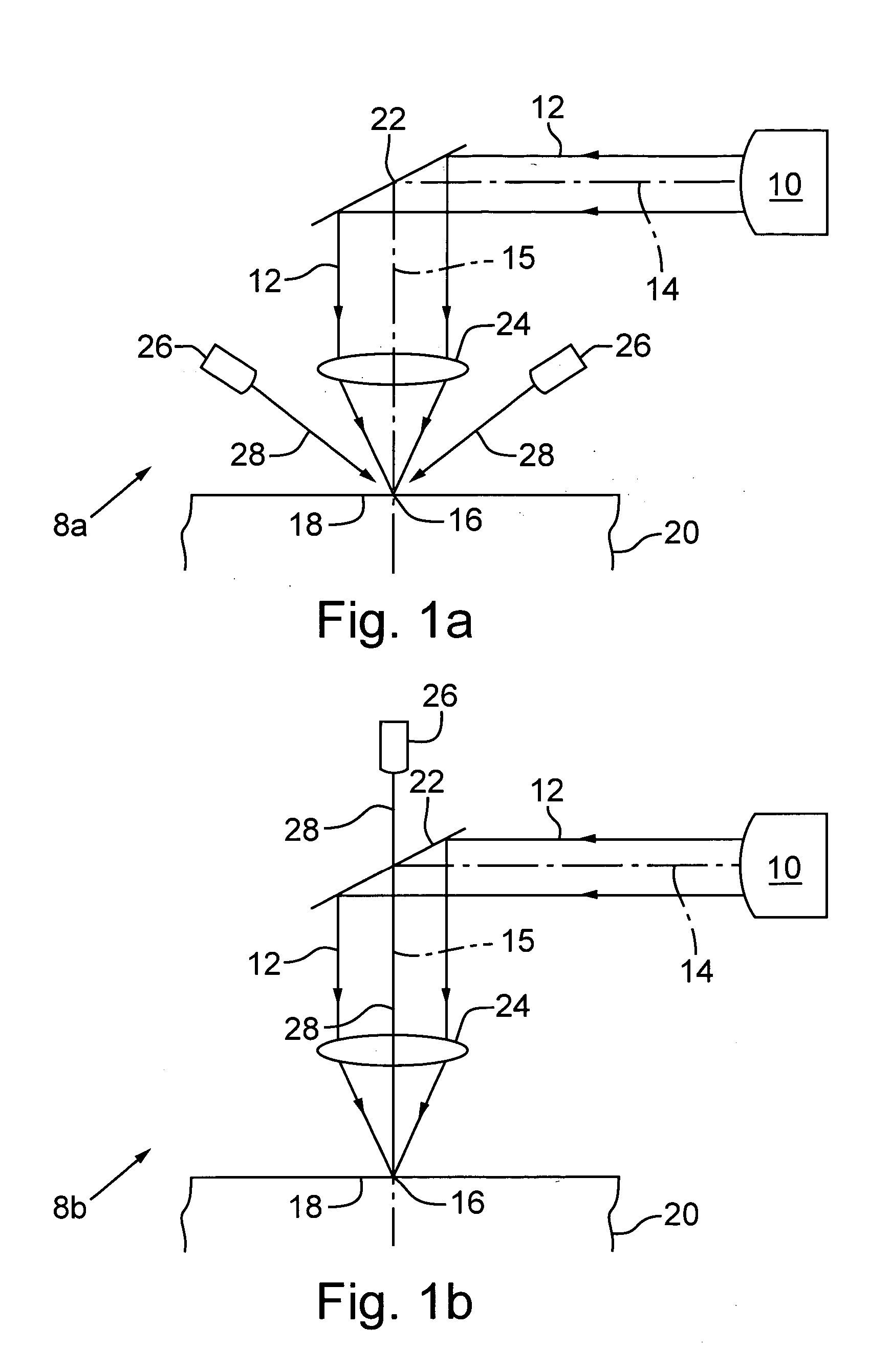
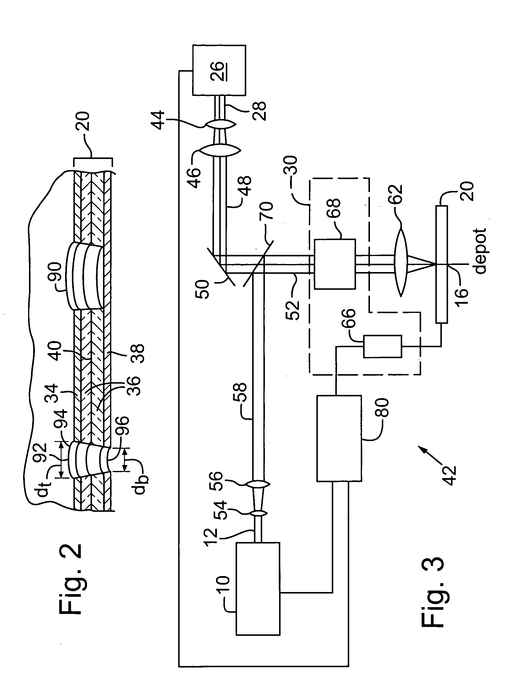
[0041] In a first preferred implementation of the first embodiment, processing laser 10 is the above-described UV DPSS laser used to effect via formation and heating source 26 is a continuous wave (CW) or quasi-CW diode laser including a laser power modulator or a diode-driving current modulator. The diode laser is preferably a single or multiple diode laser operating at a wavelength of between about 600 nm and about 1600 nm and a power level of between about 0.01 W and about 1000 W, more preferably between about 20 W and about 100 W. The CW diode laser preferably emits a laser output having a wavelength that is between about 780 nm and about 950 nm. One commercially available CW diode laser is the FC series CW diode laser with fiber coupling, a laser wavelength near 808 nm, and an output power of between about 15 W to about 30 W manufactured by Spectra-Physics of Mountain View, Calif. Another preferred heating source 26 is an array of light emitting diodes with fiber coupling, a la...

second embodiment

[0050] In a first preferred implementation of the present invention, the processing laser is a mode-locked laser generating a processing laser output having a wavelength between about 200 nm and about 1600 nm, and the heating energy is generated by at least one of the following light sources: a diode laser, a diode laser array, and a fiber laser. More specifically, the processing laser is preferably a mode-locked IR laser including optional following pulse picking and amplification and emitting a light beam having a wavelength equal to or less than about 1064 nm, a pulse width of between about 0.01 picosecond and about 1000 picoseconds, and an average laser power of between about 1 W and about 50 W at a pulse repetition rate of between about 1 kHz and about 150 MHz. An exemplary commercially available mode-locked IR laser is a Staccato laser manufactured by Lumera Laser of Chemnitz, Germany. The currently available IR power for this laser is about 20 W for a repetition rate of betwe...


PUM

PropertyMeasurementUnit
wavelengthaaaaaaaaaa

Abstract

A method and laser system effect rapid removal of material from a workpiece by applying heating energy in the form of a light beam to a target location on the workpiece to elevate its temperature while maintaining its dimensional stability. When the target portion of the workpiece is heated, a laser beam is directed for incidence on the heated target location. The laser beam preferably has a processing laser output that is appropriate to effect removal of the target material from the workpiece. The combined incidence of the processing laser output and the heating energy on the target location enables the processing laser output to remove a portion of the target material at a material removal rate that is higher than the material removal rate achievable when the target material is not heated.

Description

RELATED APPLICATIONS [0001] This application claims the benefit under 35 U.S.C. § 119(c) of U.S. Provisional Patent Application No. 60 / 514,240, filed Oct. 24, 2003.TECHNICAL FIELD [0002] The present invention relates to laser processing a locally heated workpiece and, in particular, to a system and method that elevate the temperature of a target location on the workpiece to effect an increase in target material removal rate and workpiece throughput rate. BACKGROUND OF THE INVENTION [0003] Laser processing can be conducted on numerous different workpieces using various lasers effecting a variety of processes. The specific types of laser processing of interest with regard to the present invention are laser processing of a single or multilayer workpiece to effect hole and / or via formation and laser processing of a semiconductor wafer to effect wafer dicing. [0004] Regarding laser processing via and / or holes in a multilayer workpiece, U.S. Pat. Nos. 5,593,606 and 5,841,099 of Owen et al...

Claims


Application Information

Patent Timeline
Patent Type & Authority Applications(United States)
IPC IPC(8): B23K26/06B23K26/38H05K3/00
CPCB23K26/0604B23K26/0608B23K26/381B23K26/385H05K3/0038H05K2203/108B23K26/409B23K26/4005B23K26/401B23K26/4015B23K26/402B23K26/4065B23K26/4075H05K2203/1105B23K26/40B23K26/382B23K26/389B23K2103/08B23K2103/10B23K2103/12B23K2103/14B23K2103/172B23K2103/26B23K2103/42B23K2103/50B23K2103/52B23K2103/56B23K26/00B23K26/38
Inventor SUN, YUNLONGJINJIAO, LIUHARRIS, RICHARD S.SUBRAHMANYAN, PRADEEPHAINSEY, ROBERT F.LU, WEIXIONG
Owner ELECTRO SCI IND INC
Why Eureka
Try Eureka