
Eureka
For R&D, Eureka makes reading and utilizing patents & technical documents easy.
Eureka AIR
Designed for self-driven R&D workflows. Generate viable solutions, solve complex R&D challenges, empower your innovation with AI.

Eureka Materials
Designed for material experts only. Revolutionize your material R&D, from search, analyze, to developing new materials.

TechResearch
Generate reliable direction feasibility study reports for your R&D in just a few steps.

TechSeek
Discover and master advanced knowledge NOW. Basics, ideas, possibilities, all at once.

TechMind
As an expert in R&D Theories, TechMind can generates customized viable solutions instantly.

TechRisk
Analyze your overall solution with one click, know your potential R&D risks in advance.

TechMonitor
Get weekly tech updates, stay abreast of the latest tech innovations and key insights.
Optical waveguide sensor and measuring apparatus using said optical waveguide sensor, and measuring method using a sensor
- Summary
- Abstract
- Description
- Claims
- Application Information
AI Technical Summary
Benefits of technology
Problems solved by technology
Method used
Image

Examples
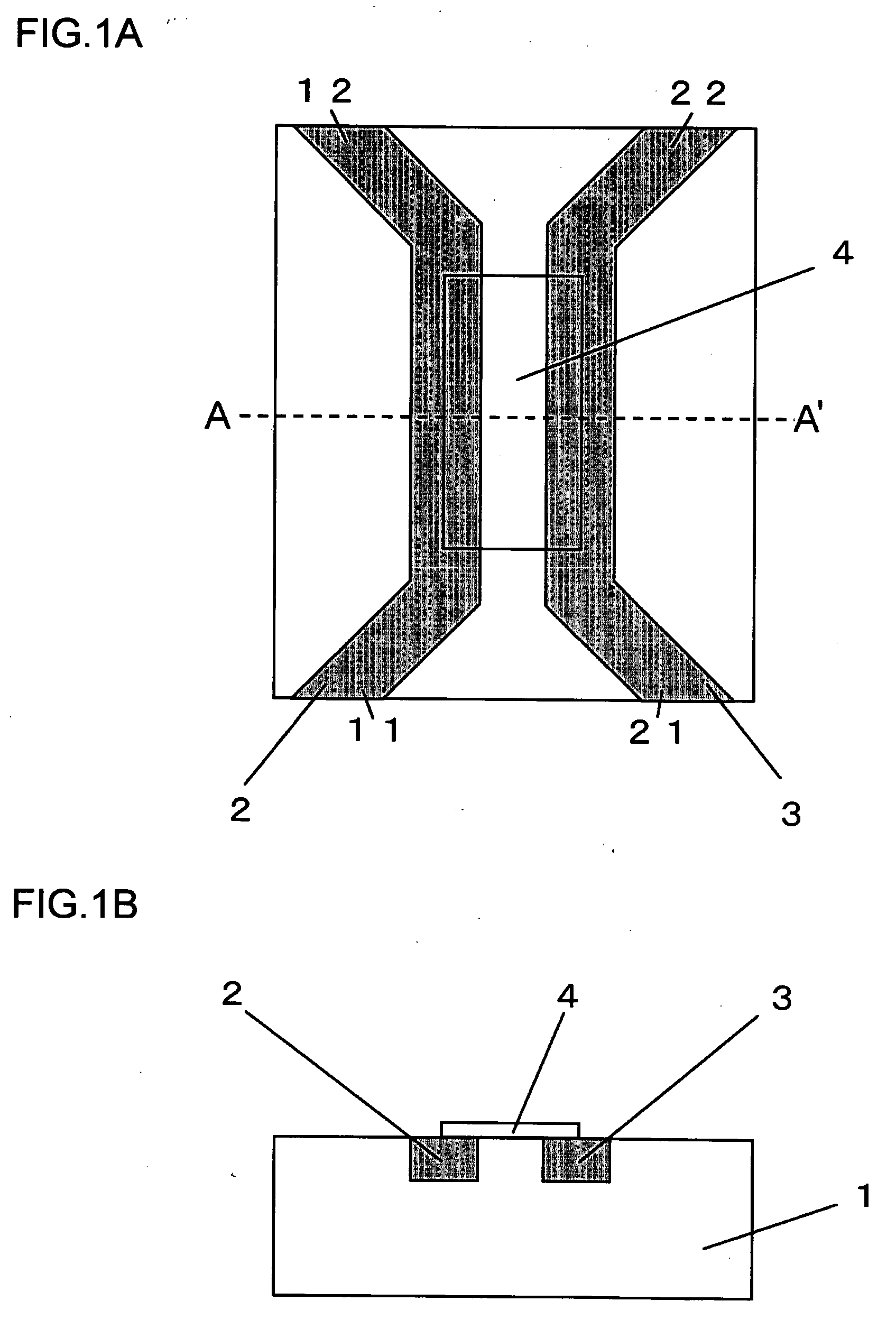
first embodiment
[0053]FIG. 1A and FIG. 1B illustrate schematically a structure of an optical waveguide sensor according to a first embodiment of the present invention. FIG. 1A is a top view of the sensor, and FIG. 1B is an A-A′ cross-sectional view of FIG. 1A. Disposed on the surface of a substrate 1, which functions as a cladding layer, are a first core layer 2 and a second core layer 3, which have a larger refractive index than the substrate 1 and serve as an optical waveguide.
[0054] As material for the substrate 1, epoxy (refractive index: 1.43-1.62) or acryl (refractive index: 1.33-1.70) may be used.
[0055] As a material for the first core layer 2 and the second core layer 3, any of the PMMA type, polycarbonate type, deuterated polymer type, fluorinated polymer type, norbornen type, polystyrene type or silicone polymer type materials may be used. In addition to these, an optical glass such as BK7 or F2 may be used.
[0056] The interval between the first core layer 2 and the second core layer 3 ...
second embodiment
[0073] A second embodiment concerns an optical waveguide sensor utilizing surface plasmon resonance and optical mode coupling.
[0074]FIG. 4A and FIG. 4B illustrate schematically a structure of an optical waveguide sensor according to a second embodiment of the present invention. FIG. 4A is a top view of the sensor, and FIG. 4B is an A-A′ cross-sectional view of FIG. 4A. The second embodiment differs from the first embodiment in that a detector 6 is disposed on top of a first core layer 2. The detector 6 is of such a structure that a receptor material, which develops an interaction with a substance to be detected, adheres to a metal thin film. As material for the metal film, a metallic material that produces surface plasmon, such as gold, silver or aluminum, is preferably used. The material usable as a receptor material and its fixing method are the same as described in the first embodiment.
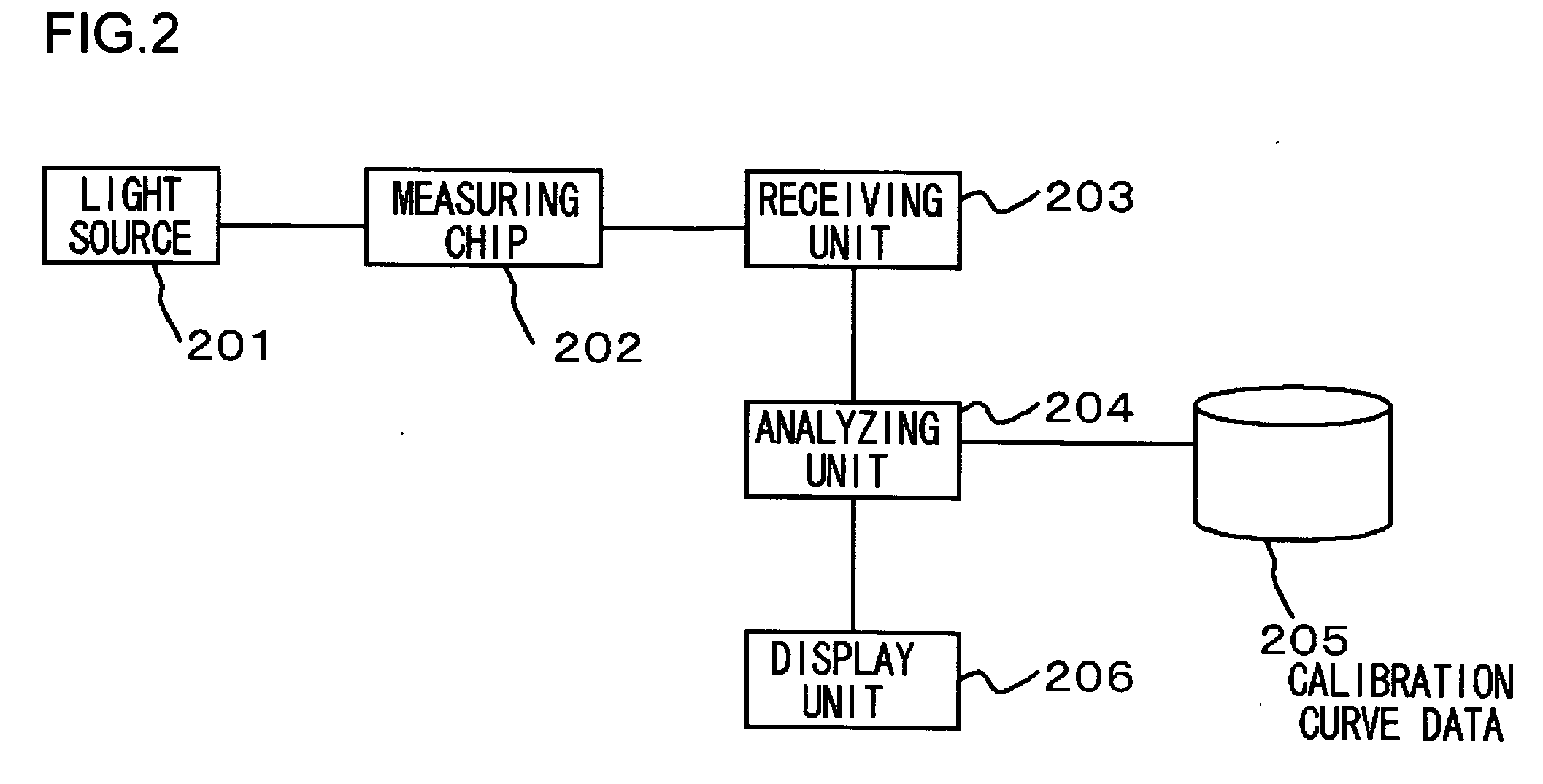
[0075] Now the principle of operation of this sensor will be described. First, lightwaves are...
third embodiment
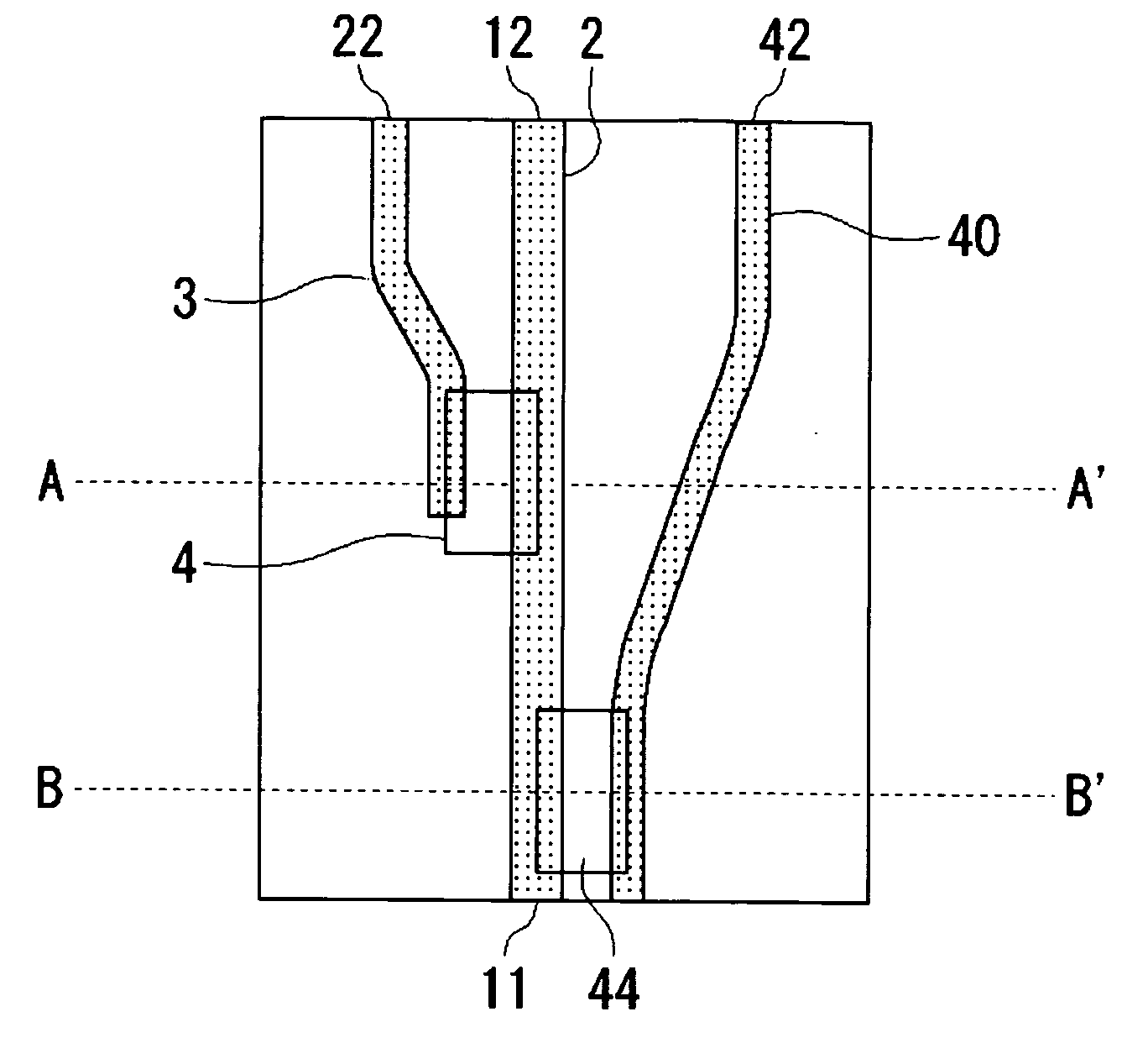
[0083] A third embodiment concerns an optical waveguide sensor utilizing surface plasmon resonance and optical mode coupling, which is suited for multiple-item measurement.
[0084]FIG. 5A and FIG. 5B illustrate schematically a structure of an optical waveguide sensor according to the third embodiment of the present invention. FIG. 5A is a cross-sectional view of the sensor, and FIG. 5B is another cross-sectional view of the sensor different from one in FIG. 5A. A second core layer 3 is disposed on the surface of a first substrate 1; a second cladding layer 5 is disposed on the surface of the second core layer 3; and a first core layer 2 is disposed on the surface of the second cladding layer 5.
[0085] A first metal thin film 7, a second metal thin film 8 and a third metal thin film 9 are disposed in parts of the surface of the first core layer 2. These metal thin films function as a detector. The first core layer 2 and the second core layer 3 are disposed counter to each other with t...
PUM
 Abstract
Description
Claims
Application Information
 - R&D Engineer
- R&D Manager
- IP Professional
- Industry Leading Data Capabilities
- Powerful AI technology
- Patent DNA Extraction
Browse by: Latest US Patents, China's latest patents, Technical Efficacy Thesaurus, Application Domain, Technology Topic, Popular Technical Reports.
© 2024 PatSnap. All rights reserved.Legal|Privacy policy|Modern Slavery Act Transparency Statement|Sitemap|About US| Contact US: help@patsnap.com