Method for manufacturing wiring, thin film transistor, light emitting device and liquid crystal display device, and droplet discharge apparatus for forming the same

a technology of light emitting devices and droplets, which is applied in the direction of static indicating devices, physical/chemical process catalysts, instruments, etc., can solve the problems of difficult to form a small wiring in width, difficult to narrow a line width (simply referred to as a width) of a wiring, and difficult to draw a continuous line in a desired region. , to achieve the effect of easy control of position

Inactive Publication Date: 2005-05-05
SEMICON ENERGY LAB CO LTD
View PDF19 Cites 119 Cited by
  • Summary
  • Abstract
  • Description
  • Claims
  • Application Information

AI Technical Summary

Benefits of technology

[0010] It is an object of the present invention to provide a method for forming a wiring which is narrower and of which position is easily controlled in forming a wiring by an ink-jet method. In addition, it is an object to provide a thin film transistor and a semiconductor device having the wiring and a manufacturing method thereof.

Problems solved by technology

In the case of forming a wiring by using an ink-jet method as described above, a droplet (a dot) discharged from an ink-jet nozzle spreads on a wiring formation surface, and it is difficult to narrow a line width (simply referred to as a width) of a wiring.
Therefore, it is difficult to draw a continuous line in a desired region.
Thus, it is difficult to form a small wiring in width and to control a position of a wiring to be formed in a designated position by an ink-jet method.

Method used


Image

  • Method for manufacturing wiring, thin film transistor, light emitting device and liquid crystal display device, and droplet discharge apparatus for forming the same
  • Method for manufacturing wiring, thin film transistor, light emitting device and liquid crystal display device, and droplet discharge apparatus for forming the same
  • Method for manufacturing wiring, thin film transistor, light emitting device and liquid crystal display device, and droplet discharge apparatus for forming the same

Examples


embodiment mode 1

[Embodiment Mode 1]

[0051] A specific method for manufacturing a wiring is described in this embodiment mode.

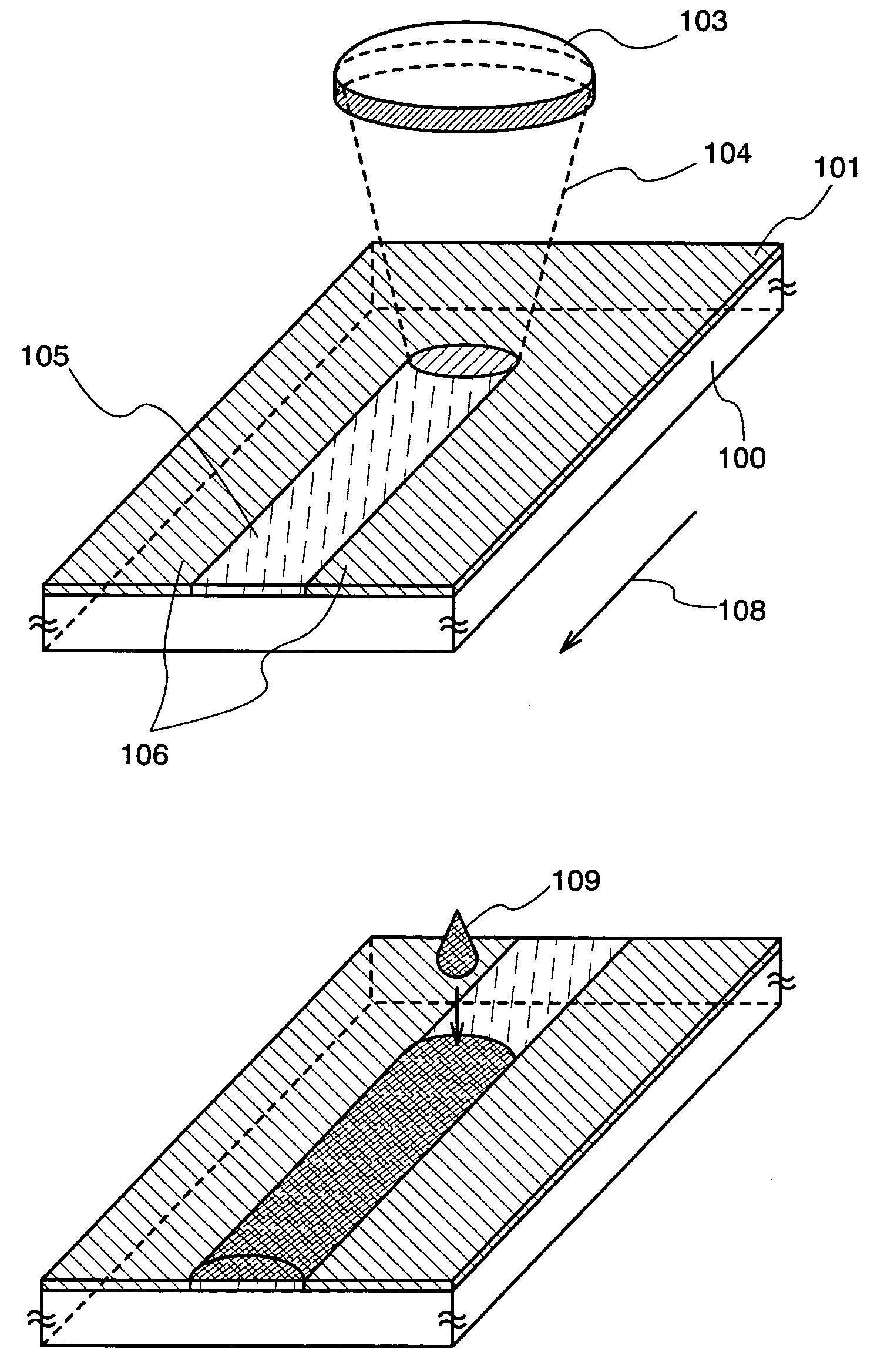
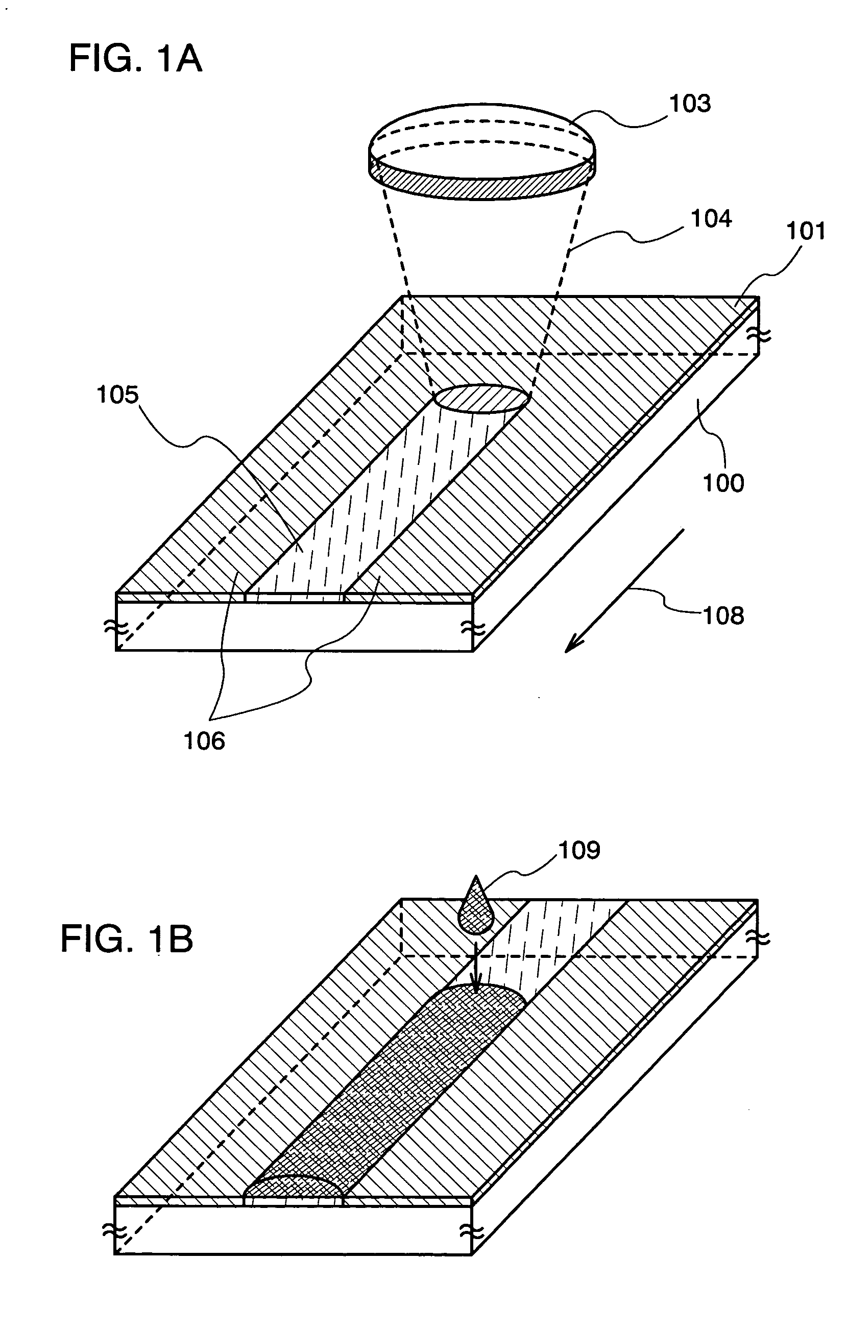
[0052] As shown in FIG. 1A, a photocatalytic substance 101 is formed over a region 100 where a wiring is to be formed. The photocatalytic substance can be formed by a dip coating method of a sol-gel method, a spin coating method, an ink-jet method, an ion plating method, an ion beam method, a CVD method, a sputtering method, an RF magnetron sputtering method, a plasma spraying method, or an anodic oxidation method. In addition, the photocatalytic substance can be formed by mixing and melting a salt of a constituent element, in the case of a photocatalytic substance made of an oxide semiconductor including a plurality of metals. A solvent may be baked or dried when it is necessary to remove the solvent in the case of forming the photocatalytic substance by an application method such as a dip coating method or a spin coating method. Specifically, it may be heated at a predeterm...

embodiment mode 2

[Embodiment Mode 2]

[0076] The case of using an oil (alcohol) based solvent as a solvent of a conductive material is described in this embodiment mode.

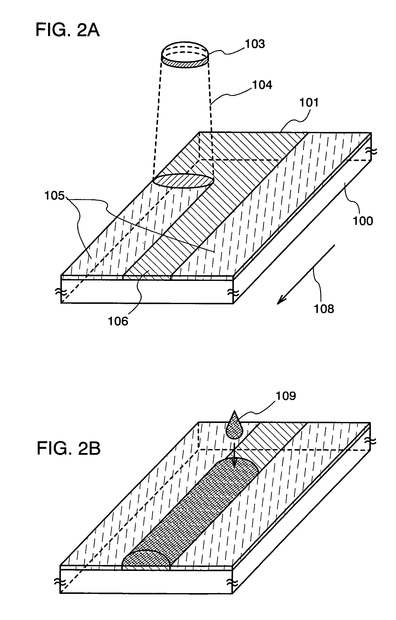
[0077] A photocatalytic substance 101 is formed over a region 100 where a wiring is to be formed as described in Embodiment Mode land as shown in FIG. 2A. Subsequently, light is converged by using an optical system to selectively irradiate with light. For example, light irradiation is selectively performed by converging light 104 with a lens 103 and relatively moving TiO2 and the light. For example, the photocatalytic substance 101 may be moved in a direction of an arrow 108. Accordingly, an irradiation region 105 and a non-irradiation region 106 can be formed. Then, TiO2 in the irradiation region 105 shows an oil-repellent property.

[0078] Thereafter, a dot 109 is discharged from above the non-irradiation region as shown in FIG. 2B. An oil (alcohol) based solvent is used as the solvent of the conductive material in this embodiment mo...

embodiment mode 3

[Embodiment Mode 3]

[0085] An example of forming a thin film transistor by using a method for manufacturing a wiring described in the above embodiment mode is described in this embodiment mode. Note that TiO2 is used as a photocatalytic substance.

[0086] First, a base film 201 is formed over a substrate 200 having an insulating surface (over an insulating surface) as shown in FIG. 3A. A glass substrate such as barium borosilicate glass or aluminoborosilicate glass, a quartz substrate, a stainless steel substrate, or the like can be used as the substrate 200. Although a substrate made of a flexible synthetic resin such as plastics typified by polyethylene-terephthalate (PET), polyethylenenaphthalate (PEN), or polyeter sulfone (PES) or acrlyic generally tends to have a lower heat resistance temperature compared to other substrates, it can be used as the substrate 200 as long as it can withstand the process temperature in the manufacturing step.

[0087] The base film 201 is formed in ord...


PUM

PropertyMeasurementUnit
contact angleaaaaaaaaaa

Abstract

As a semiconductor device, specifically, a pixel portion included in a semiconductor device is made to have higher precision and higher aperture ratio, it is required to form a smaller wiring in width. In the case of forming a wiring by using an ink-jet method, a dot spreads on a wiring formation surface, and it is difficult to narrow width of a wiring. In the present invention, a photocatalytic substance typified by TiO2 is formed on a wiring formation surface, and a wiring is formed by utilizing photocatalytic activity of the photocatalytic substance. According to the present invention, a narrower wiring, that is, a smaller wiring in width than a diameter of a dot formed by an ink-jet method can be formed.

Description

BACKGROUND OF THE INVENTION [0001] 1. Field of the Invention [0002] The present invention relates to a method for manufacturing a wiring and a method for manufacturing a semiconductor device such as a light emitting device or a liquid crystal display device by a droplet discharge (ink-jet) method utilizing a photocatalytic reaction. In addition, the invention relates to a droplet discharge apparatus for forming them. [0003] 2. Related Art [0004] A droplet discharge technique typified by a piezo method or a thermal jet method, or a continuous droplet discharge technique has attracted attention. This droplet discharge technique has been used in printing a type and drawing an image. However, an attempt to apply it to a semiconductor field, for example, micropattern formation or the like has begun in recent years. [0005] On the other hand, there is a method for forming a patterned metal film made of only an absorption metal atom by soaking a base material provided with a substance havin...

Claims


Application Information

Patent Timeline
Patent Type & Authority Applications(United States)
IPC IPC(8): B01J35/02B05D3/00B05D5/12C08J7/18G02F1/1368G21H1/00H01L21/027H01L21/28H01L21/288H01L21/3205H01L21/336H01L21/768H01L27/32H01L29/786H01L51/00H01L51/56
CPCG09G2300/0814H01L21/288H01L21/76838H01L27/3244H01L2251/5323H01L51/0022H01L51/56H01L2251/5315H01L27/3276H10K59/12H10K71/611H10K59/131H10K2102/3031H10K2102/3026H10K71/00
Inventor NAKAMURA, OSAMUOGINO, KIYOFUMI
Owner SEMICON ENERGY LAB CO LTD
Why Eureka
Try Eureka