Composite material, wafer holding member and method for manufacturing the same

a technology of holding member and composite material, which is applied in the direction of woodworking apparatus, turning machine accessories, chucks, etc., can solve the problems of not being able to meet the requirements of a single factor of he leakage rate, the vacuum gas tightness of conventional composite materials cannot be maintained at 1.310sup>10 /sup>pam, and the plate base is cracked, etc., to achieve excellent thermal conductivity, small variation in strength, and high vacuum gas

Inactive Publication Date: 2005-05-12
KYOCERA CORP
View PDF13 Cites 17 Cited by
  • Summary
  • Abstract
  • Description
  • Claims
  • Application Information

AI Technical Summary

Benefits of technology

[0023] An object of the present invention is to provide a composite material, which has a higher vacuum gas-tightness, an excellent thermal conductivity, an adjustable coefficient of thermal expansion, small variation in strength and higher reliability, and a method for manufacturing the composite material, and a wafer holding member including the composite material.

Problems solved by technology

However, since the above-mentioned composite plate, composed either of two components of Al and SiC or of Al, Si and SiC, is porous itself, when the plate base serving as a wafer holding member and the plate are joined to each other using a brazing material or solder, it cannot maintain vacuum gas-tightness of 1.3×10⁻¹⁰ Pa·m3 / sec or below in terms of He leak rate, which is required for a semiconductor manufacturing apparatus.
The conventional composite material cannot simultaneously satisfy all the factors of He leak rate, variation in strength, thermal conductivity and coefficient of thermal expansion.
A wafer holding member, in which a plate base and a plate of Al are joined to each other using Al-brazing or In-brazing in order to increase the thermal conductivity, has a problem that the plate base is cracked under a thermal shock cycle of −40 to 100 degree-C., which is required for a deposition apparatus, such as CVD, PVD and sputtering, or an etching apparatus, because of the large difference in coefficient of thermal expansion between the plate of Al and the plate base.
Furthermore, when the composite plate, composed of two components of aluminum and SiC, and the ceramic plate are joined to each other using metal, wetting between the aluminum and the metal joint layer is not so good.
Even though the composite plate of two components and the ceramic plate are integrated using metal joint, pores are likely to be created in the joint interface because of the bad wetting between the metal joint layer and the aluminum.
In case metal is used for the joint material, wetting between the aluminum and the metal joint material is bad, resulting in minute pores created between the metal joint material and the aluminum.
It is difficult to maintain the reliability under the thermal shock cycle.
But there is a problem on residual attracting force, that a force for attracting the wafer remains because electric charges, which have been accumulated on the placing surface 20a after applying voltage to the electrode 20 for electrostatic attraction to attract the wafer to the placing surface 24a and then turning off the applied voltage to release the wafer on completion of a deposition or etching process, is not neutralized immediately.
While the residual attracting force emerges, there are some problems that the wafer cannot be released even in an effort to put the wafer off the placing surface 20a, positioning of the wafer is out of order if released, or at its worst, the wafer is broken when the wafer is forced to be released form the placing surface.

Method used


Image

  • Composite material, wafer holding member and method for manufacturing the same
  • Composite material, wafer holding member and method for manufacturing the same
  • Composite material, wafer holding member and method for manufacturing the same

Examples


embodiment 1

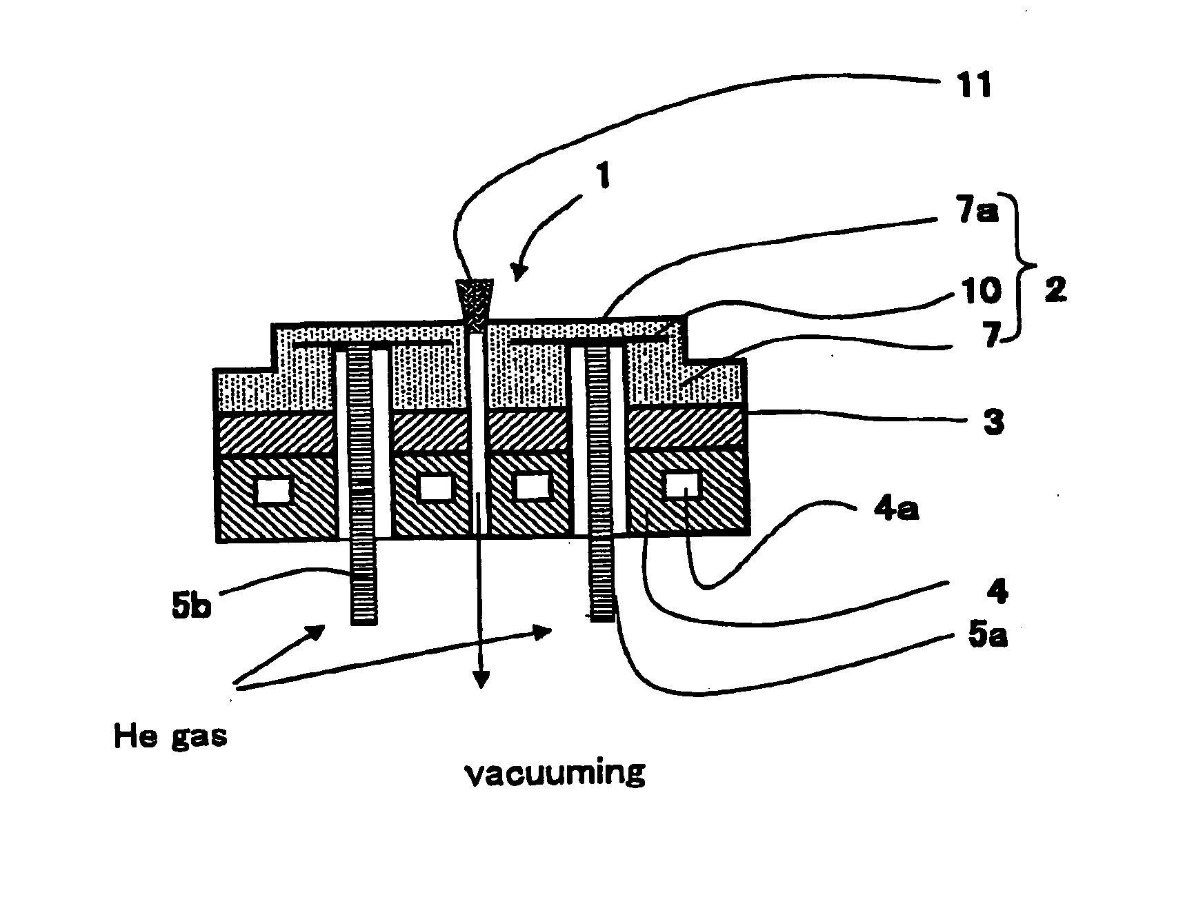
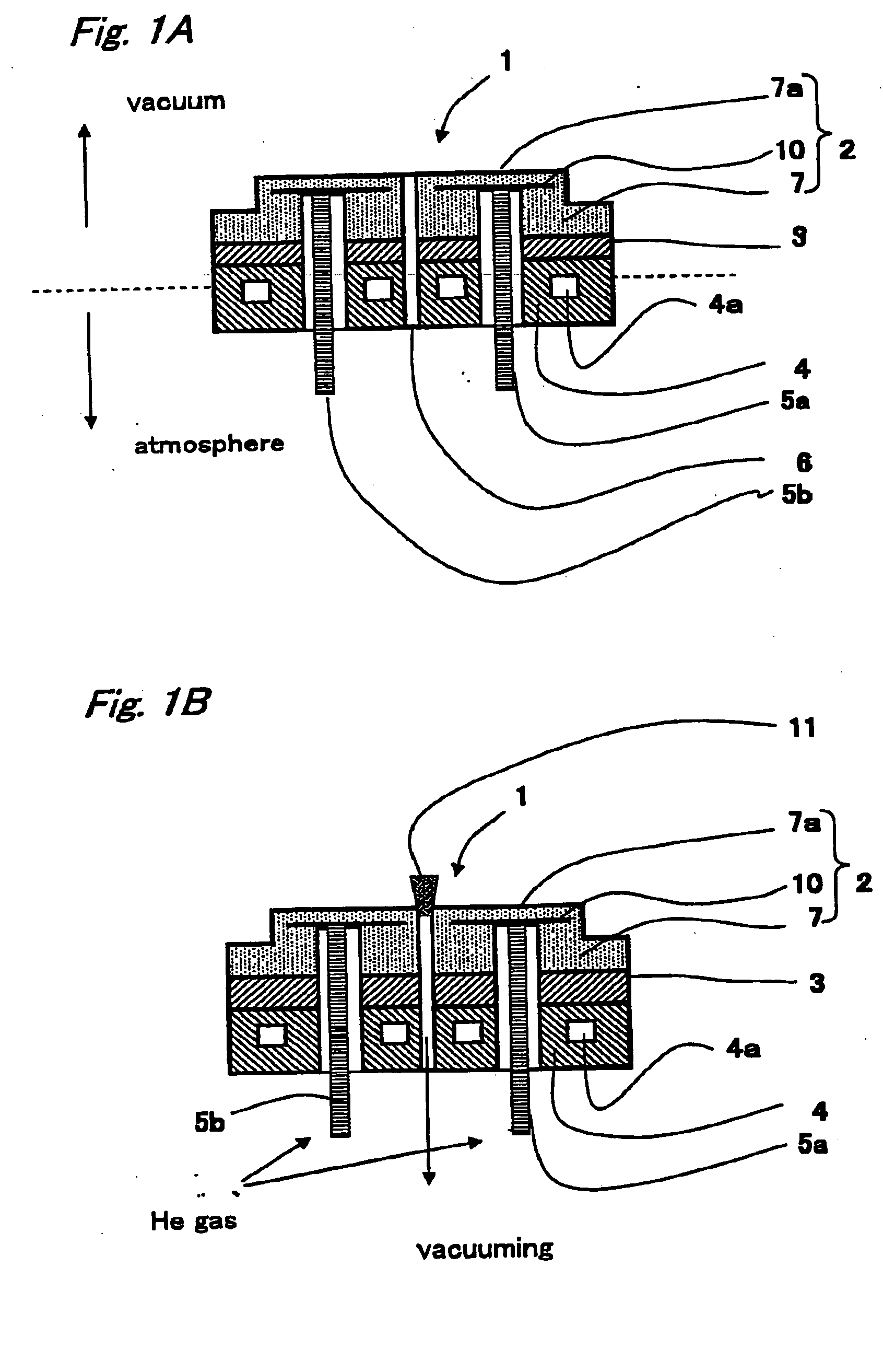
[0065]FIG. 1A is a sectional view showing the first embodiment of the present invention. FIG. 1B is a explanatory view showing a measurement method of a leak rate.

[0066] A wafer holding member 1 includes a wafer holding portion 2 having a plate base 7, one principal plane of which serves as a placing surface 7a for mounting a wafer, and electrodes 10 provided either on the other principal plane or inside of the plate base 7; and a plate 4 composed of SiC, SiO2, and at least one out of Al and Si, wherein the wafer holding portion 2 and the plate 4 are joined to each other via a metal joint material 3 on a face opposite to the placing surface 7a of the wafer holding portion 2.

[0067] The plate base 7 is preferably formed of oxide ceramics, such as alumina, nitride ceramics, carbide ceramics. On the placing surface 7a, provided is a groove (not shown). When an argon gas of the like is supplied through a gas feeding hole 6 passing through the wafer holding portion 2, a space between a ...

embodiment 2

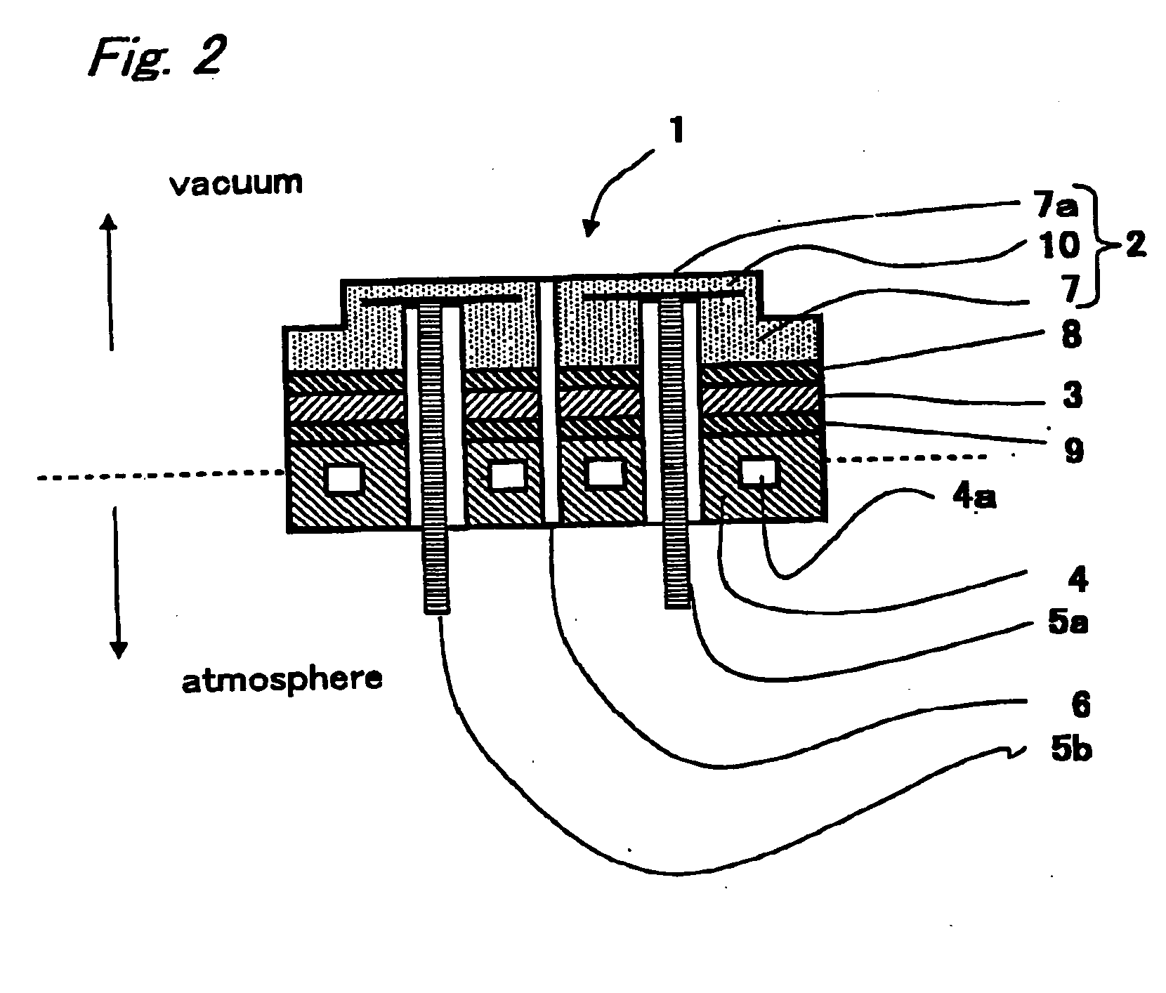
[0106]FIG. 2 is a sectional view showing the second embodiment of the present invention, and FIG. 3 is a plan view thereof.

[0107] The wafer holding member 1 includes a wafer holding portion 2a having a plate ceramic body 7, one principal plane of which serves as a placing surface 7a for mounting a wafer, and an electrode 10 provided either on the other principal plane or inside of the plate ceramic body 7, a composite plate 4 containing SiC, aluminum and silicon, a metal layer 8 provided on a face opposite to the placing surface 7a of the wafer holding portion 2, and a metal layer 9 provided on a face of the composite plate 4, wherein the wafer holding portion 2 and the composite plate 4 are joined to each other via a metal joint material 3 between the metal layers 8 and 9.

[0108] The plate ceramic body 7 is preferably formed of oxide ceramics, such as alumina, nitride ceramics, carbide ceramics. On the placing surface 7a, provided is a groove (not shown). When an argon gas of the ...

example 1

[0142] A fusion solidified body containing 74 mass % of SiC, 15.6 mass % of Al, 10.4 mass % of Si, and another solidified body containing 84.4 mass % of SiC, 15.6 mass % of Al, 0 mass % of Si, and the other solidified body containing 89.6 mass % of SiC, 0 mass % of Al, 10.4 mass % of Si, were produced. Then, while changing time of soaking each of the fusion solidified bodies in ethyl silicate, each composite material having a different content of SiO2 was produced. The produced composite material had dimensions of 50 mm×50 mm×5 mm.

[0143] Then, each He leak rate was measured. Measurement of He leak rate included steps of finishing the surface of the above-mentioned composite material up to a roughness of Ra 0.1 to 0.2 μm using diamond powder of 5 μm, followed by attaching the surface of the composite material with a metal pipe integrated with an O-ring having an internal diameter of 30 mm and an external diameter of 34 mm, followed by vacuuming the inside room of the pipe, followed ...


PUM

PropertyMeasurementUnit
mass %aaaaaaaaaa
mass %aaaaaaaaaa
mass %aaaaaaaaaa

Abstract

A composite material according to the present invention, is composed of SiC, SiO2, at least one out of Al and Si, with He leak rate of 1.3×10⁻¹⁰ Pa·m3/sec or below, thereby providing a composite material, which has a higher vacuum air-tightness, an excellent thermal conductivity, an adjustable coefficient of thermal expansion, small variation in strength and higher reliability, and a method for manufacturing the composite material, and a wafer holding member including the composite material.

Description

BACKGROUND OF THE INVENTION [0001] 1. Field of the Invention [0002] The present invention relates to a composite material, which is composed of a ceramic component and a metallic component, and a method for manufacturing the composite material and a wafer holding member including the composite material. The present invention also relates to a wafer holding member for holding a wafer, such as semiconductor substrate or a substrate for liquid crystal, either in a deposition process, such as CVD (Chemical Vapor Deposition), PVD (Physical Vapor Deposition), sputtering, SOD (Spin-on Dielectric), SOG (Spin-on Glass), or in an etching process, and a method for manufacturing the wafer holding member. [0003] 2. Description of the Related Art [0004] A composite material composed of a metal and a ceramics has characteristics that a coefficient of thermal expansion can be optionally adjusted by changing the ratio of metal to ceramics, with a desired thermal conductivity by selecting metallic sp...

Claims


Application Information

Patent Timeline
Patent Type & Authority Applications(United States)
IPC IPC(8): H01L21/68B32B18/00C04B35/565C04B35/581C04B35/653C04B37/02C23C16/458H01L21/00H01L21/02
CPCB32B18/00Y10T279/23B32B2315/02C04B35/565C04B35/581C04B35/6261C04B35/62625C04B35/6264C04B35/653C04B37/026C04B2235/3225C04B2235/3229C04B2235/3409C04B2235/3418C04B2235/402C04B2235/404C04B2235/428C04B2235/6025C04B2235/6581C04B2235/72C04B2235/80C04B2235/96C04B2235/9607C04B2235/963C04B2237/12C04B2237/121C04B2237/365C04B2237/40C04B2237/402C04B2237/403C04B2237/405C04B2237/407C04B2237/408C04B2237/64C23C16/4581C23C16/4586H01L21/67103H01L2924/0002B32B2311/20Y10T428/12597Y10T428/12576H01L2924/00H01L21/02H01L21/68
Inventor YOKOYAMA, KIYOSHIITONAGA, NAOKO
Owner KYOCERA CORP
Why Eureka
Try Eureka