Charge-trapping memory device and methods for operating and manufacturing the cell

a memory device and charge-trapping technology, applied in semiconductor devices, transistors, instruments, etc., can solve the problems of not being able to shrink the cell to sub-100 nm technology, deteriorating the performance of the memory cell with an increasing number of programming cycles, and not being advantageous for scalability, so as to achieve less degradation, improve reliability, and reduce the amount of charge injected in the single gate dielectric above the middle channel region.

Inactive Publication Date: 2005-05-19
POLARIS INNOVATIONS
View PDF12 Cites 41 Cited by
  • Summary
  • Abstract
  • Description
  • Claims
  • Application Information

AI Technical Summary

Benefits of technology

[0006] In the case of silicon nitride, the equivalent oxide thickness due to the value of the relative permittivity or relative dielectric constant, is about half as much as the real physical thickness. A nitride layer, which is, for example, 10 nm thick is equivalent to a silicon dioxide layer, which is about 5 nm thick. The electric field strength is the derivative of the voltage along the selected paths. This value has to be maintained larger across the charge-trapping strips than across the single gate dielectric above the middle channel region. In this way, the amount of charge injected in the single gate dielectric above the mid...

Problems solved by technology

Therefore, it is not possible to shrink the cell to the sub-100-nm technology since the increasing amount of charges in the middle channel region cannot be completely neutralized during the reprogramming process.
Thus, the performance of the memory cell will deteriorate with a...

Method used


Image

  • Charge-trapping memory device and methods for operating and manufacturing the cell
  • Charge-trapping memory device and methods for operating and manufacturing the cell
  • Charge-trapping memory device and methods for operating and manufacturing the cell

Examples


Embodiment Construction

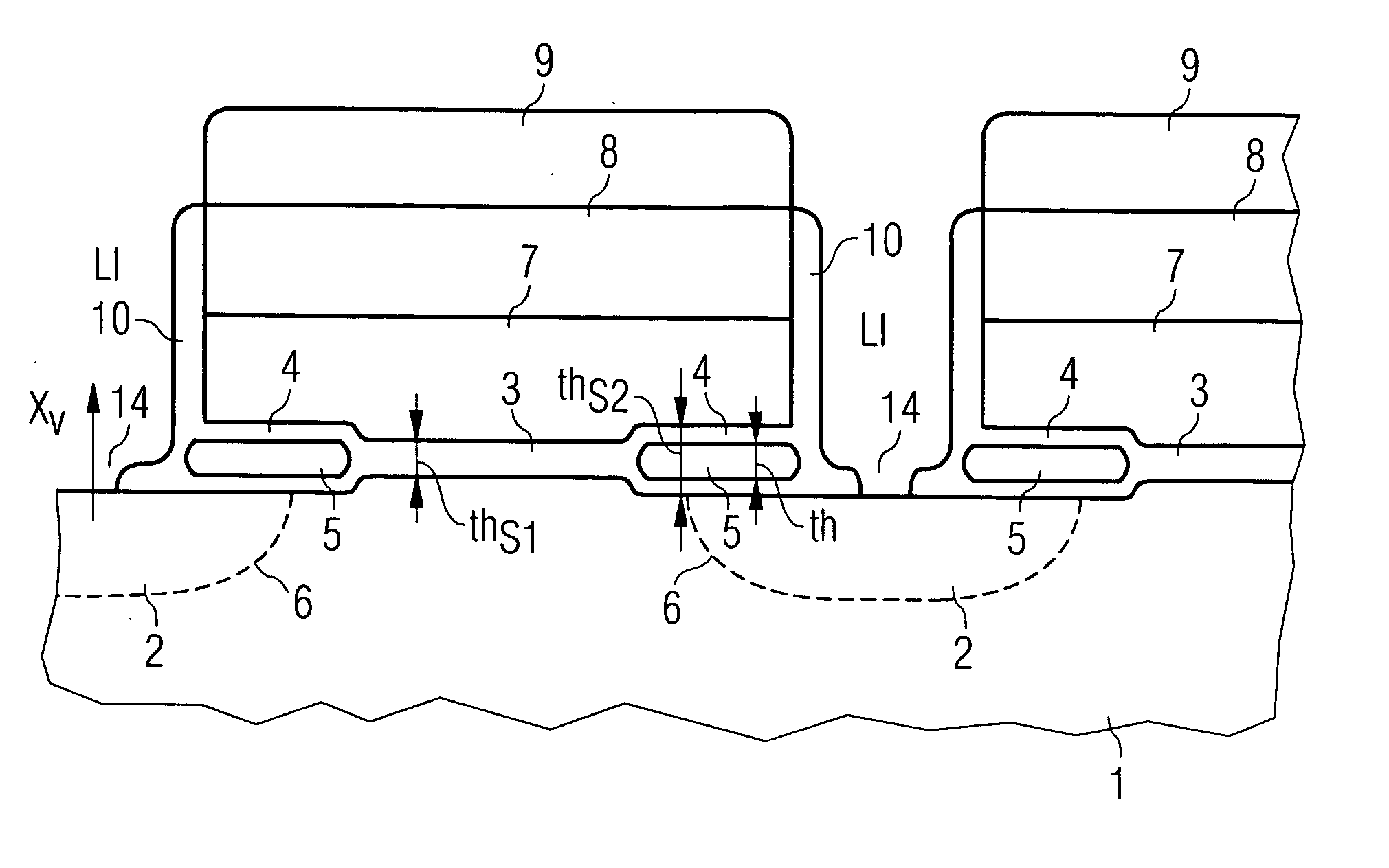
[0022]FIG. 1 shows a cross-section of a preferred embodiment of the memory device. In a semiconductor body 1 or substrate, preferably p-doped, source and drain regions 2 are formed by doped regions, preferably n+-doped. A gate dielectric 3 is arranged on an upper surface of said semiconductor body 1. The gate dielectric 3 is a single layer above a middle section of a channel region located between source and drain regions of the same memory cell. At both ends of the channel, the gate dielectric is structured as a charge-trapping layer sequence 4 comprising a charge-trapping layer 5 formed by two strips 5 of a material having a higher relative permittivity or relative dielectric constant than the material of the gate dielectric 3. For example, if the gate dielectric is silicon dioxide, the material of the charge-trapping layer 5 can be silicon nitride. The strips of the charge-trapping layer 5 are located above upper boundaries of junctions 6 that are designated by dotted lines in FI...


PUM


Abstract

The charge-trapping layer comprises two strips above the source and drain junctions. The thicknesses of the charge-trapping layer and the gate dielectric are chosen to facilitate Fowler-Nordheim-tunnelling of electrons into the strips during an erasure process. Programming is performed by injection of hot holes into the strips individually for two-bit storage.

Description

TECHNICAL FIELD [0001] The invention generally relates to semiconductor memory devices and more particularly to charge-trapping memory devices. BACKGROUND [0002] Memory devices with charge-trapping layers, especially SONOS memory cells comprising oxide-nitride-oxide layer sequences as storage medium, are usually programmed by channel hot electron injection. U.S. Pat. No. 5,768,192 and U.S. Pat. No. 6,011,725 disclose charge-trapping memory cells of a special type of so-called NROM cells, which can be used to store bits of information both at the source and at the drain below the respective gate edges. The programmed cell is read in reverse mode to achieve a sufficient two-bit separation. Erasure is performed by hot hole injection. The current consumption of each cell during programming with fully driven transistor is about 100 μA. An increment of charges towards the middle channel region significantly reduces the number of possible programming cycles. Therefore, it is not possible t...

Claims


Application Information

Patent Timeline
IPC IPC(8): G11C16/04H01L21/28H01L21/8246H01L27/115H01L29/792
CPCG11C16/0466G11C16/0491H01L29/7923H01L27/115H01L27/11568H01L21/28282H01L29/40117H10B69/00H10B43/30
Inventor MIKOLAJICK, THOMASREISINGER, HANSWILLER, JOSEFLIAW, CORVIN
Owner POLARIS INNOVATIONS
Why Eureka
Try Eureka