Semiconductor texturing process
a technology of semiconductors and texturing processes, applied in the direction of solid-state devices, cable/conductor manufacturing, basic electric elements, etc., can solve the problems of increased carrier recombination at the silicon surface, inability to use the method, and high cost of techniques
- Summary
- Abstract
- Description
- Claims
- Application Information
AI Technical Summary
Benefits of technology
Problems solved by technology
Method used
Image

Examples
example 1
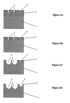
[0054] A silicon nitride layer approximately 2 nm thick was deposited on a polished silicon wafer of (111) orientation. A sample was cut out of the wafer and etched in a solution of 1:50 hydrofluoric acid:nitric acid at 0° C. The sample was encapsulated behind 1 mm thick low iron glass using silicone and its reflectance was measured using a spectrophotometer with an integrating sphere. The sample had a reflectivity of 11% at 900 nm, while a polished encapsulated silicon reference wafer had a reflectivity of 24% and a sample of (100) oriented silicon textured with inverted pyramids had a reflectivity, of 8% at the same wavelength. These results indicate that the texturing process is very effective at reducing reflection from the silicon surface.
example 2
Etching of Thin Silicon Strips
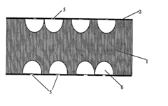
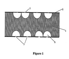
[0055] A 100 mm diameter, 1 mm thick, (110) oriented silicon wafer was used. Thin silicon strips spaced 105 microns apart and approximately 70 microns thick were produced in the wafer, following the processes described in International Patent Application no. WO 02 / 45143. The sidewalls of the thin silicon strips so produced are highly polished. It was desired to texture the sidewalls as they would form the sunward facing surfaces in a solar cell.
[0056] A thin layer of silicon nitride was deposited on the wafer. One of the thin silicon strips was broken out of the wafer and mounted on the wafer surface. In this way, the sidewall surface of one of the silicon strips was clearly visible during the etching process. After a period of approximately 5 minutes etching at room temperature with the same etchant described in Example 1, the strips had textured optimally and etching was terminated. The silicon strips were now approximately 65 microns thick.
[0057] ...
example 3
Surface Passivation
[0058] Several (111) oriented, >1000 ohm-cm, boron doped float-zoned silicon wafers were used. An oxide approximately 30 nm thick was thermally grown on the wafers. A thin layer of silicon nitride was then deposited and the wafers were textured as described in Example 2. Following texturing, the wafers were given a phosphorus diffusion and a 30 nm thick oxide was thermally grown. The wafers were then given an anneal in a mixture of 5% hydrogen and 95% nitrogen at 430° C. for 30 minutes. The emitter saturation current density following these treatments was measured to be 20-25 fA / cm2 per side. This low value indicates that excellent surface passivation can be achieved on the textured surfaces.
PUM
| Property | Measurement | Unit |
|---|---|---|
| Length | aaaaa | aaaaa |
| Width | aaaaa | aaaaa |
| Width | aaaaa | aaaaa |
Abstract
Description
Claims
Application Information