

Method to form a robust TiCI4 based CVD TiN film
a tici4-based, robust technology, applied in the direction of coating, chemical vapor deposition coating, metallic material coating process, etc., can solve the problems of reducing device performance, reducing the efficiency of cvd method, and ineffective technique in reducing chloride concentration to an acceptable level for advanced technologies, etc., to achieve the effect of lowering resistivity and stress
- Summary
- Abstract
- Description
- Claims
- Application Information
AI Technical Summary
Benefits of technology
Problems solved by technology
Method used
Image

Examples
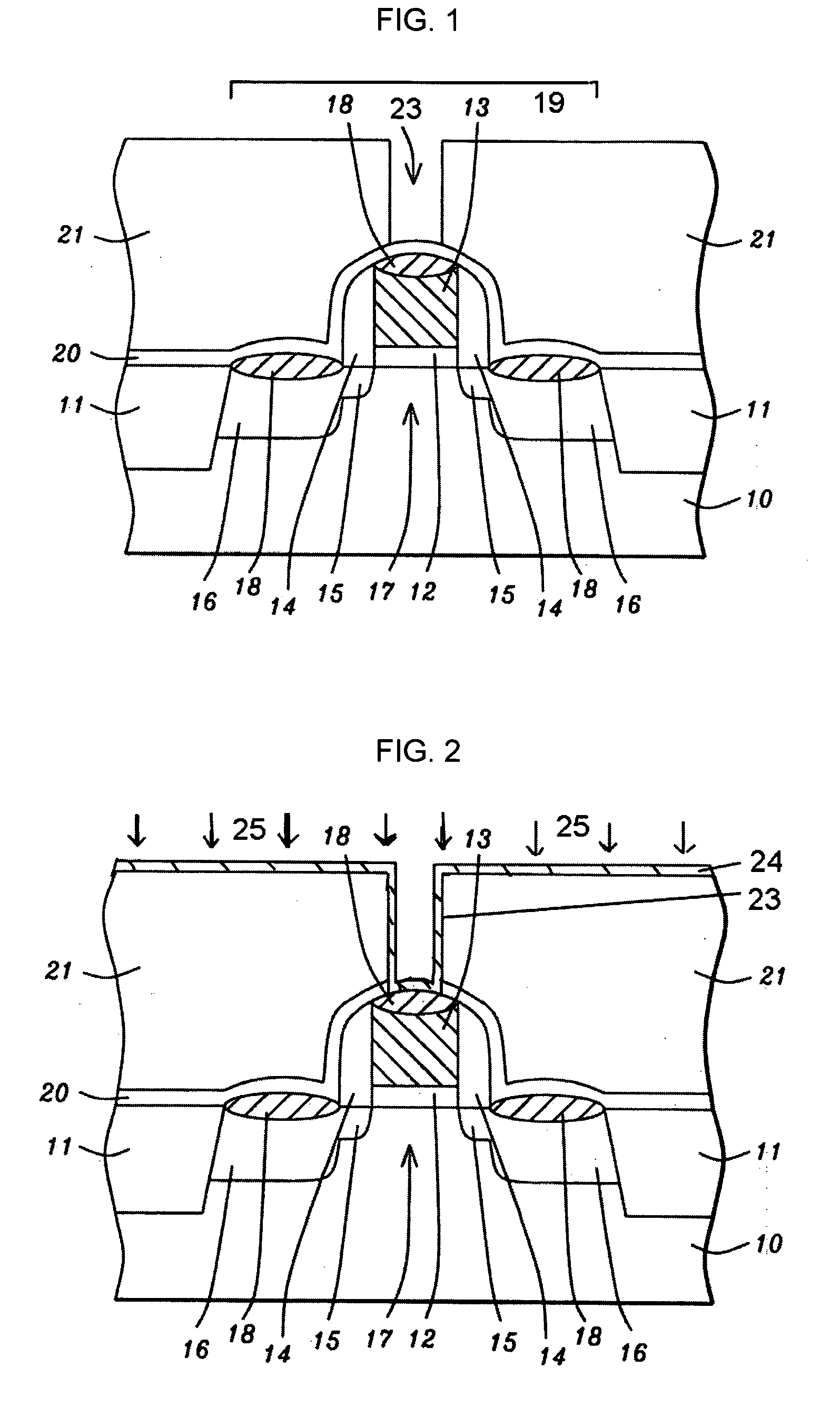
first embodiment
[0035] A further advantage of the plasma treatment 25 of the present invention is that it imparts improved film stability to the transformed TiN layer 24a. For example, when the samples in Table 1 were exposed to ambient (air) for a period of time (q-time) that varied between 0 and 48 hours, the resistivity for TiN layer 24 increased from 306 μOhm-cm at t=0 to 322 μOhm-cm after 48 hours which is an increase of 5.2%. During a similar period of 48 hours, the transformed TiN layer 24a had a stable 158μOhm-cm resistivity with a 0% increase. Presumably, the resistivity increase for the untreated TiN layer 24 is due to a surface oxidation to form a titanium oxide layer. Stability as a function of q-time is graphically expressed in FIG. 8 where a TiN layer that has not been subjected to a N-containing plasma treatment experiences an increase in resistivity (curve 40) while a TiN layer treated by a method shows a stable resistivity (line 41).
[0036] Returning to FIG. 3, a conventional seque...
second embodiment
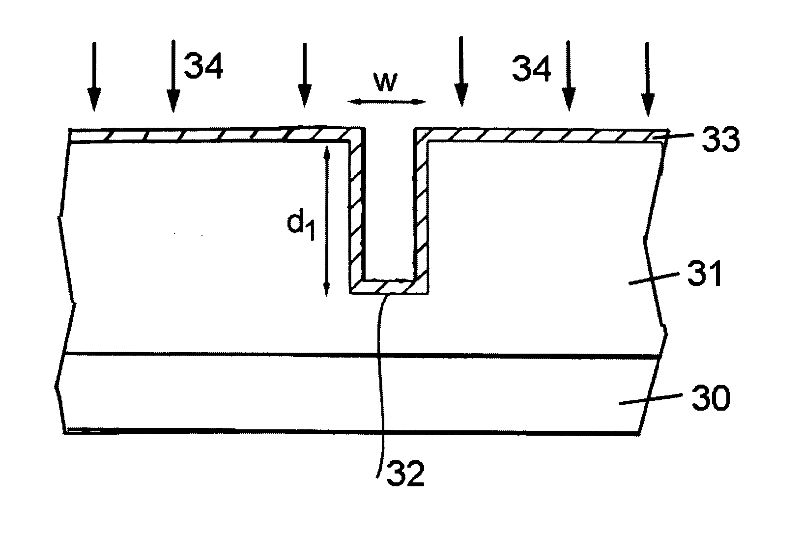
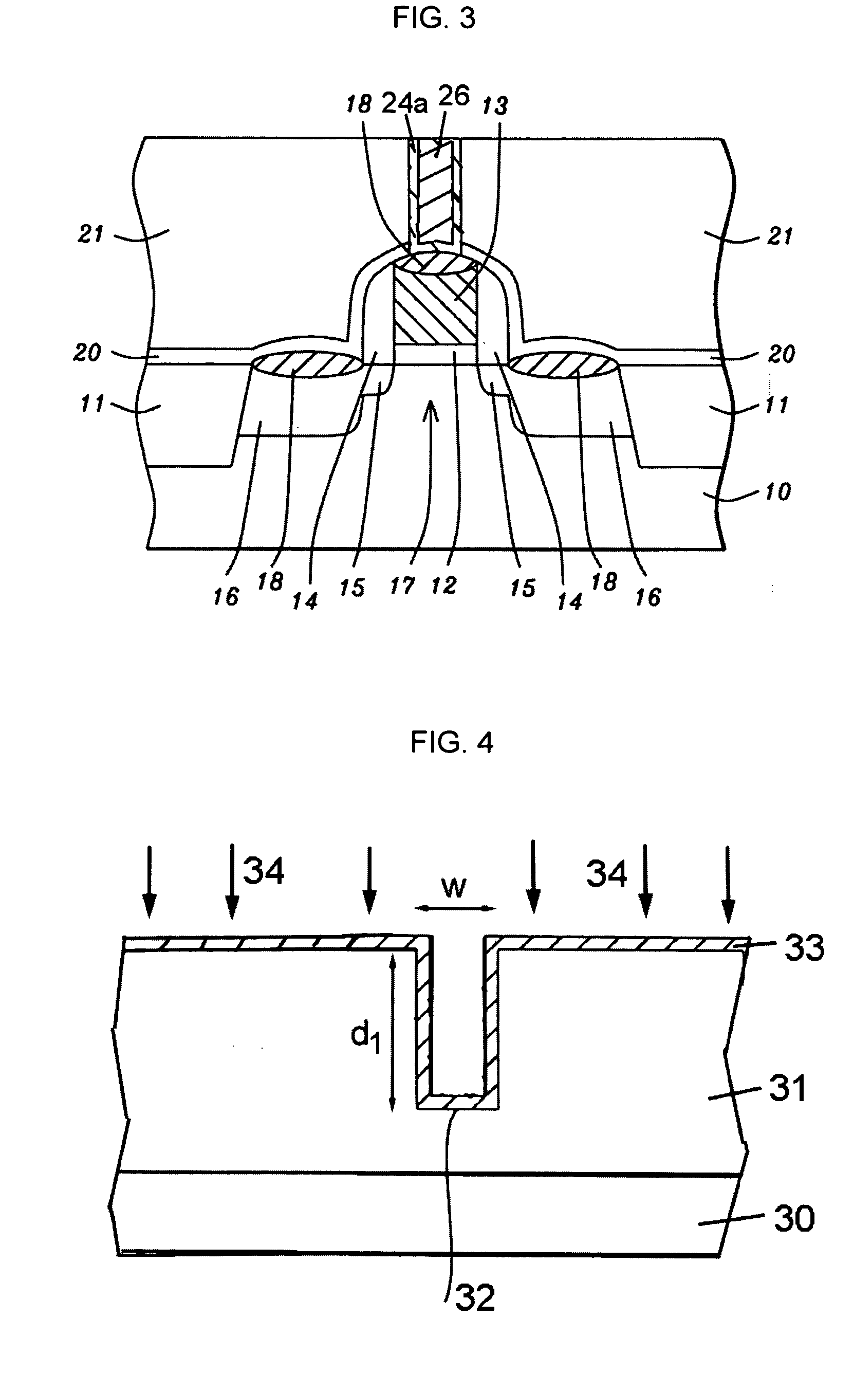
[0037] In a second embodiment depicted in FIGS. 4-7, the present invention is employed to form a TiN layer which serves as a bottom electrode in a MIM capacitor. Referring to FIG. 4, a substrate 30 is provided that is typically silicon but may optionally be based on Si—Ge, SiGeC, Ga—As or other semiconductor materials employed in the art. A dielectric layer 31 having a thickness from about 2000 to 20000 Angstroms is then deposited on the substrate 30 by a CVD, PECVD, or spin-on method. The dielectric layer 31 is comprised of SiO2 or a low k dielectric material such as fluorine doped SiO2, carbon doped SiO2, a polysilsesquioxane, a poly(arylether), fluorinated polyimide, or benzocyclobutene. Additional processing may follow such as an anneal or plasma treatment step to densify the dielectric layer 31. Furthermore, a planarization step may be employed to form a smooth surface on the dielectric layer 31 which will improve the process latitude of a subsequent patterning step.
[0038] A co...
PUM
| Property | Measurement | Unit |
|---|---|---|
| Temperature | aaaaa | aaaaa |
| Temperature | aaaaa | aaaaa |
| Time | aaaaa | aaaaa |
Abstract
Description
Claims
Application Information