Piezoelectric element, fabrication method for the same, and inkjet head, inkjet recording apparatus and angular velocity sensor including the same

a fabrication method and piezoelectric element technology, applied in the field of piezoelectric elements, can solve the problems of further larger piezoelectric displacement, mgo monocrystal, and high material cost, and achieve high durability, high piezoelectric properties, and high piezoelectric properties.

Active Publication Date: 2005-06-16
PANASONIC CORP
View PDF4 Cites 25 Cited by
  • Summary
  • Abstract
  • Description
  • Claims
  • Application Information

AI Technical Summary

Benefits of technology

[0040] According to this invention, since the adhesion between the first electrode film and the first piezoelectric film is high, a piezoelectric element having high piezoelectric properties and high durability can be realized. Also, according to the method for fabricating a piezoelectric element of this invention, piezoelectric elements having high piezoelectric properties and high durability can be easily mass produced. Furthermore, the present invention provides a highly reliable inkjet head with minimized variation in discharging an ink and an inkjet recording apparatus including the inkjet head.
[0041] Moreover, the present invention provides highly reliable thin angular velocity sensors that can be easily mass produced.

Problems solved by technology

The MgO monocrystal is, however, a very expensive material, and therefore, this method is not preferred from the viewpoint of cost when it is applied to mass production of industrial products of piezoelectric elements using the piezoelectric thin film.
Also, when a high voltage is applied to the piezoelectric thin film, further larger piezoelectric displacement can be caused.
When a high voltage is applied to an actuator in which a PZT film is formed by the sputtering not requiring the post annealing in the aforementioned manner, however, film peeling is disadvantageously caused between a film used as the underlying electrode and the perovskite type oxide film.
Therefore, such an actuator has insufficient durability as a piezoelectric actuator for causing large displacement.

Method used


Image

  • Piezoelectric element, fabrication method for the same, and inkjet head, inkjet recording apparatus and angular velocity sensor including the same
  • Piezoelectric element, fabrication method for the same, and inkjet head, inkjet recording apparatus and angular velocity sensor including the same
  • Piezoelectric element, fabrication method for the same, and inkjet head, inkjet recording apparatus and angular velocity sensor including the same

Examples


embodiment 1

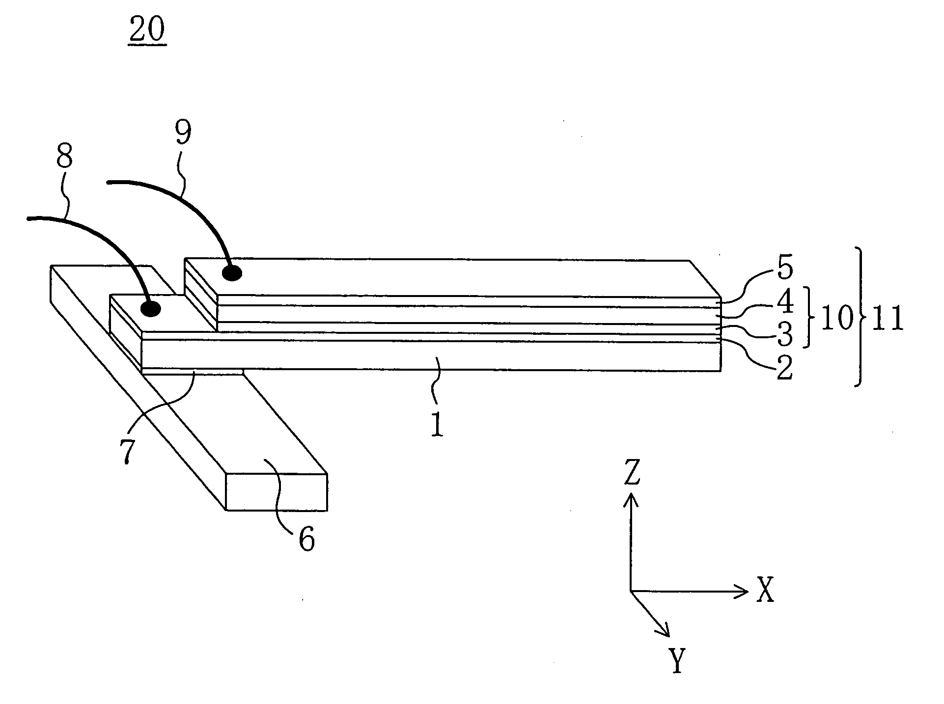
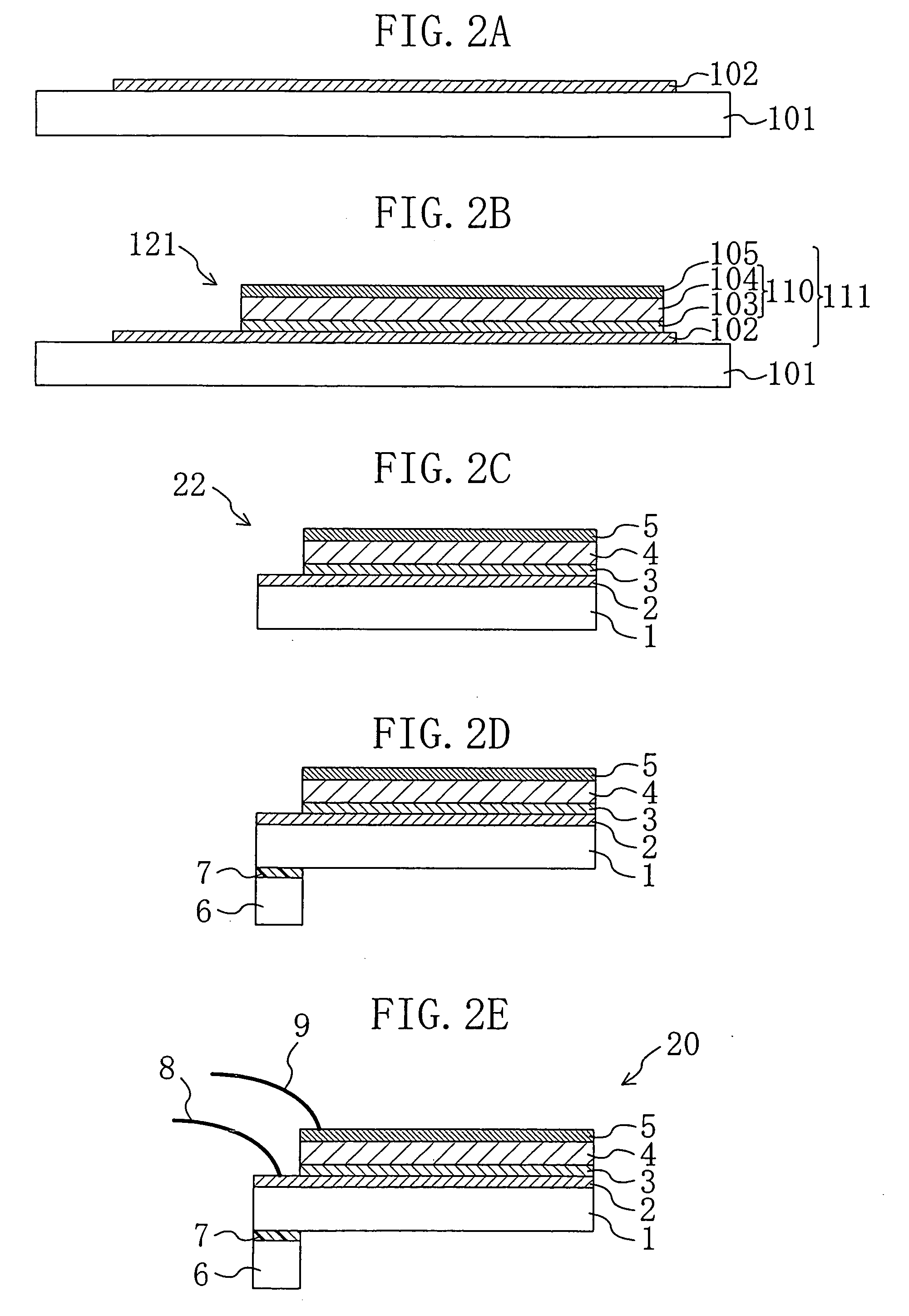
[0063] A piezoelectric element 20 according to Embodiment 1 of the invention includes, as shown in FIG. 1, a substrate 1 in the shape of a strip (with a thickness of 0.30 mm, a width of 3.0 mm and a length of 15.0 mm) and a layered body 11 formed on the substrate 1. The piezoelectric element 20 has a width of 3.0 mm. One end portion along the longitudinal direction of the piezoelectric element 20 (that is, the left end portion in FIG. 1) is fixed on a stainless steel supporting substrate 6 (with a thickness of 1.0 mm, a width of 3.0 mm and a length of 10.0 mm) with an epoxy resin adhesive 7. The end portion herein means a portion with a length of 3.0 mm from the end of the piezoelectric element 20 (that is, the left end in FIG. 1). The longitudinal direction of the piezoelectric element 20 is substantially perpendicular to the longitudinal direction of the stainless steel supporting substrate 6. Thus, the piezoelectric element 20 is constructed as a cantilever.

[0064] The substrate ...

example 1

[0082] In this example, a silicon substrate was used as the substrate 101 and an iridium (Ir) thin film with a thickness of 100 nm was used as the first electrode film 102. This iridium thin film was deposited by using a ternary rf-magnetron sputtering system. Specifically, the silicon substrate 101 was previously annealed to 400° C. and the temperature was kept. A mixed gas of argon and oxygen (with a gas volume ratio of Ar:O2 of 15:1) was used as a sputtering gas and a total gas pressure was kept at 0.25 Pa. Iridium was used as a first target of the ternary magnetron sputtering system. The sputtering was performed for 960 seconds under application of high frequency power of 200 W, thereby depositing the iridium thin film (without using second and third targets).

[0083] The thickness of the piezoelectric layered film 110 was set to 3550 nm. The piezoelectric layered film 110 was composed of a first piezoelectric film 103 with a thickness of 50 nm made of lead zirconate titanate (he...

example 2

[0093] In this example, a Pyrex glass substrate with resistance to high temperature was used as the substrate 101 and a platinum (Pt) thin film with a thickness of 150 nm was used as the first electrode film 102. This platinum thin film was deposited by using a ternary rf-magnetron sputtering system. Specifically, the Pyrex glass substrate 101 was previously annealed to 400° C. and the temperature was kept. A mixed gas of argon and oxygen (with a gas volume ratio of Ar:O2 of 15:1) was used as a sputtering gas and a total gas pressure was kept at 0.25 Pa. Platinum was used as a first target of the ternary magnetron sputtering system. The sputtering was performed for 1080 seconds under application of high frequency power of 200 W, thereby depositing the platinum thin film (without using second and third targets).

[0094] The thickness of the piezoelectric layered film 110 was set to 5100 nm. The piezoelectric layered film 110 was composed of a first piezoelectric film 103 with a thickn...


PUM


Abstract

A piezoelectric element includes a first electrode; a piezoelectric layered film composed of a first piezoelectric film formed on the first electrode film and a second piezoelectric film that is formed on the first piezoelectric film and is controlled in crystal orientation thereof by the first piezoelectric film; and a second electrode film formed on the second piezoelectric film. Each of the first and second piezoelectric films is an aggregate of columnar grains grown unidirectionally along a thickness direction of the piezoelectric layered film. A columnar grain of the second piezoelectric film has a larger cross-sectional diameter than a columnar grain of the first piezoelectric film. A ratio l/d of the thickness l of the piezoelectric layered film to the cross-sectional diameter d of the second piezoelectric film is not less than 20 and not more than 60.

Description

BACKGROUND OF THE INVENTION [0001] The present invention relates to a piezoelectric element, a fabrication method for the piezoelectric element, and an inkjet head, an inkjet recording apparatus and an angular velocity sensor including the piezoelectric element. [0002] A piezoelectric material converts mechanical energy into electric energy or electric energy into mechanical energy. A typical example of the piezoelectric material is lead zirconate titanate (Pb(Zr,Ti)O3) (hereinafter referred to as “PZT”), that is, an oxide with a perovskite type crystal structure. In using the PZT with a tetragonal crystal structure in particular, the maximum piezoelectric displacement can be obtained along the <001> axis direction (i.e., the c-axis direction). However, most of the piezoelectric materials are polycrystals of aggregates of grains, and the crystal axes of the respective grains extend in various directions. Accordingly, the directions of the spontaneous polarizations Ps are vario...

Claims


Application Information

Patent Timeline
Patent Type & Authority Applications(United States)
IPC IPC(8): B41J2/055B41J2/045B41J2/135B41J2/14B41J2/16G01C19/56G01C19/5628H01L29/84H01L41/08H01L41/09H01L41/18H01L41/22H01L41/29H01L41/316H01L41/319H01L41/39H02N2/00
CPCB41J2/14233C04B35/472C04B2235/3206C04B2235/3213C04B2235/3227C04B2235/3262H01L41/0973G01C19/5621G01C19/5628H01L41/1876H01L41/316H01L41/0815H01L41/094C04B2235/787H10N30/10516H10N30/2042H10N30/2047H10N30/8554H10N30/076H01L29/84
Inventor TORII, HIDEOFUJII, EIJIKAMADA, TAKESHIFUJII, SATORU
Owner PANASONIC CORP
Why Eureka
Try Eureka