Method for the fabrication of periodically poled Lithium Niobate and Lithium Tantalate nonlinear optical components

a nonlinear optical component and lithium tantalate technology, applied in the field of process for the fabrication of lino3 and litao3 optical devices, can solve the problems of slow and complicated growth process of sln or slt, no data on uniform optical parameters, and complex physics of domain formation in ln and lt ferroelecric crystals, etc., to reduce the influence of domain growth, slow the growth rate of domain growth, and increase the growth rate of nucleation rate ra

Active Publication Date: 2005-06-23
OOO SPECTRALUS +1
View PDF3 Cites 23 Cited by
  • Summary
  • Abstract
  • Description
  • Claims
  • Application Information

AI Technical Summary

Benefits of technology

[0025] Establishing the effect of the screening process, the depolarization and local (internal) field on domain kinetics is of great significance for progress in PPD structure engineering. The depolarization field slows the domain growth while the screening process reduces its influence.
[0026] To accomplish the objects and advantages of the present invention a novel process for the fabrication of a PPD structure from congruent LN and LT ferroelectric crystalline wafers which have been coated with stoichiometric LN or LTN thin-films having an electrode and in some embodiments an insulator structure is described. The method allows an increase in the growth rate of nucleation for reverse domains during a forward poling stage, and a decrease in the coercive field by optimizing the polarization screening and backswitching processes. The ability to control and optimize these parameters during the poling process allows one to produce a PPD structure in CLN and CLT ferroelectric crystals with small feature sizes and a high uniformity through a large area of the wafer.

Problems solved by technology

The physics of domain formation in LN and LT ferroelecric crystals is complicated.
However, the growth process for SLN or SLT is slow and complicated, a stress free bule has a maximum diameter of only about 50mm., and there are no data on uniformity of optical parameters for wafers fabricated therefrom.

Method used


Image

  • Method for the fabrication of periodically poled Lithium Niobate and Lithium Tantalate nonlinear optical components
  • Method for the fabrication of periodically poled Lithium Niobate and Lithium Tantalate nonlinear optical components
  • Method for the fabrication of periodically poled Lithium Niobate and Lithium Tantalate nonlinear optical components

Examples


Embodiment Construction

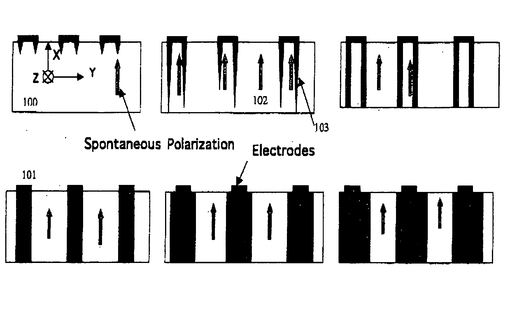
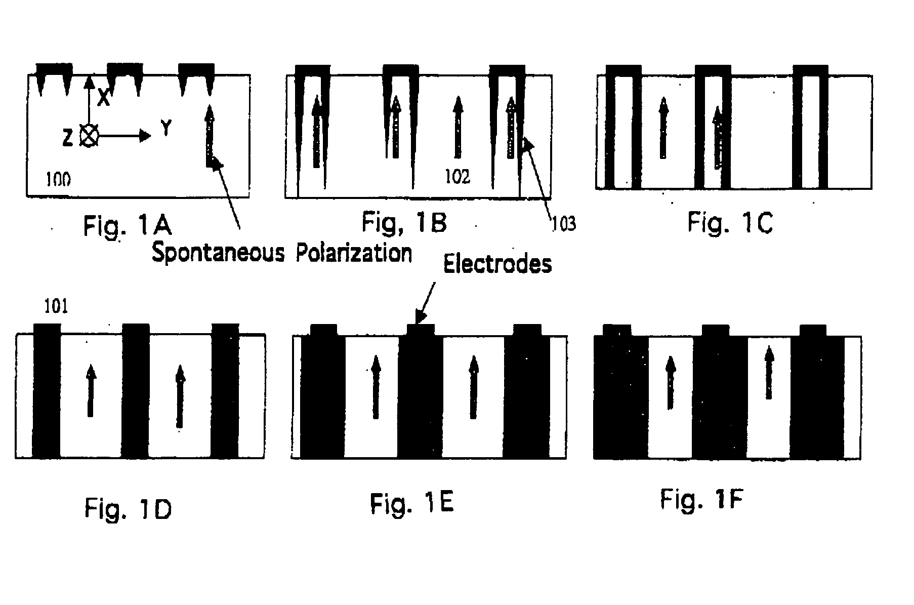
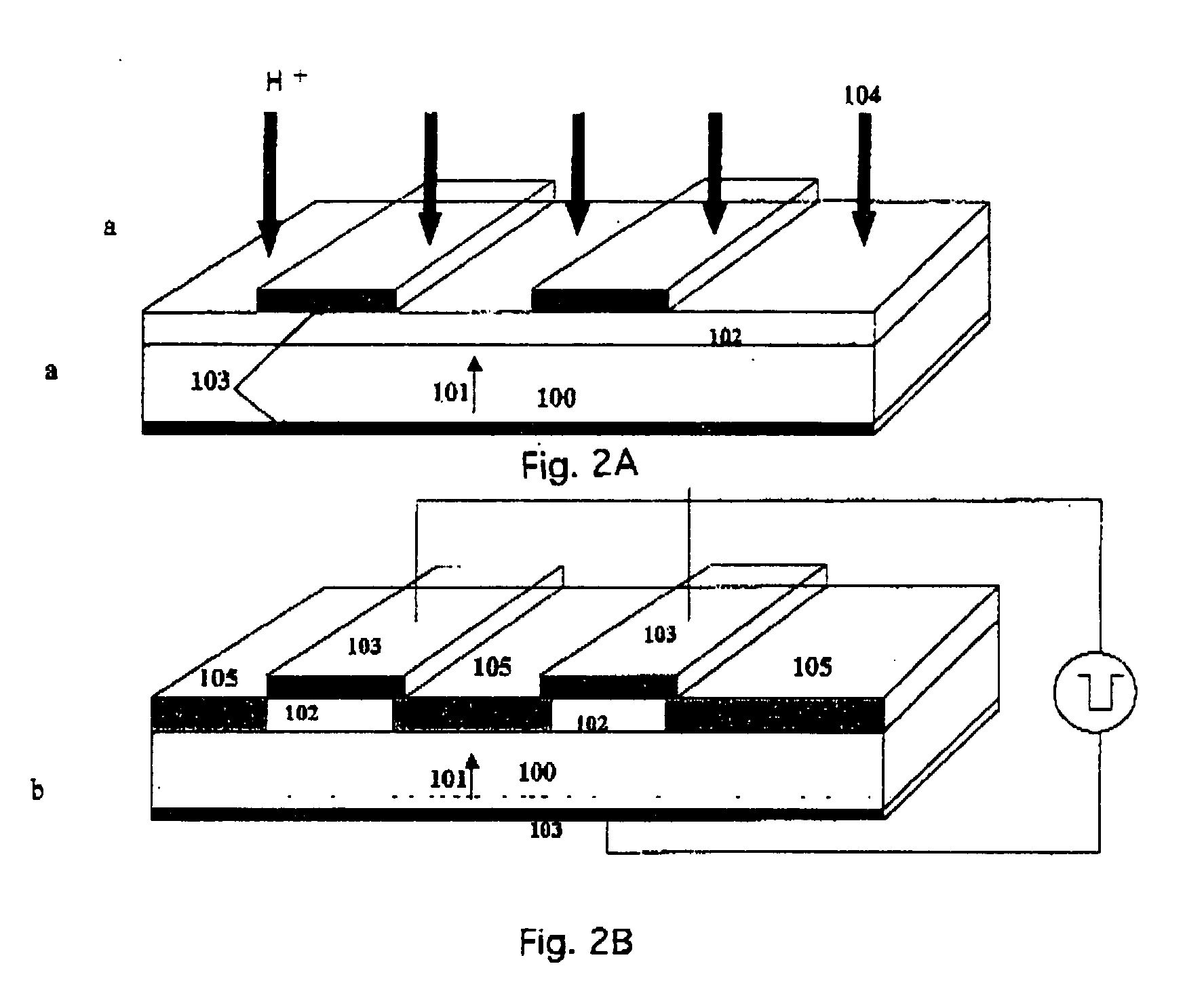
[0041] The process and product of the present invention are explained in greater detail below with reference to FIGS. 2-5. Referring first to FIGS. 2a and 2b, a single-domain congruent LN or LT wafer (substrate) 100 has a natural polarization direction as shown by the arrow 101. To obtain a sharp and defect-free interface between the deposited SLN or SLT film and the congruent LN or LT wafer substrate, a pre-deposition cleaning process of the wafer is preferably carried out, for example, by oxygen plasma washing. Next, a, for example, 0.2 μm thick SLN or SLT film (102) is deposited, preferably by the sol-gel process.

[0042] I have found that the after the crystallization of the film at, for example, 450° C., a single crystal stoichiometric film is formed in a single-domain state with its polarization in the same direction as that of the substrate.

[0043] Ta films, 0.1 μm thick (103), deposited, for example by plasma vapor sputtering (PVD)can be used as electrodes. The Ta film on the...


PUM

PropertyMeasurementUnit
thicknessaaaaaaaaaa
thicknessaaaaaaaaaa
temperatureaaaaaaaaaa

Abstract

A process for reducing the poling field of congruent grown LiNbO3 and LiTaO3 crystal-based nonlinear optical devices and for the production of domain structures with precise reproducibility of the main parameters by depositing a thin layer of a stechiometric LiNbO3 film on the Z-face of a congruent LiNbO3 or LiTaO3 wafer. A new domain nucleation, evolution and stabilization process is provided to afford a uniform, short period domain superstructure for the conversion of near infra-red light to near ultraviolet, blue and green light

Description

FIELD OF THE INVENTION [0001] This invention relates to an improved process for the fabrication of LiNO3 and LiTaO3 optical devices BACKGROUND OF THE INVENTION [0002] Since the invention of the first laser many years ago, the frequency conversion off laser radiation by nonlinear optical crystals has become an important technique widely used in quantum electronics and laser physics for solving various scientific and engineering problems. The fundamental physics of three-wave light interactions in nonlinear optical crystals is now reasonably well understood. This has enabled the production of various harmonic generators, sum- and difference-frequency generators, and optical parametric oscillators based on the nonlinear optical crystals that are now commercially available. At the same time, scientists continue an active search for improved nonlinear optical materials. The present invention relates to a method for the fabrication of a bulk periodically poled domain (PPD) structure-in co...

Claims


Application Information

Patent Timeline
Patent Type & Authority Applications(United States)
IPC IPC(8): G02F1/355
CPCG02F2202/20G02F1/3558
Inventor ESSEIAN, STEPAN
Owner OOO SPECTRALUS
Why Eureka
Try Eureka