Process for producing polymer optical waveguide

Inactive Publication Date: 2005-06-23
FUJIFILM BUSINESS INNOVATION CORP
View PDF11 Cites 32 Cited by
  • Summary
  • Abstract
  • Description
  • Claims
  • Application Information

AI Technical Summary

Benefits of technology

[0060] Examples of the rigid substrate include a film substrate, a ceramic-resin compound substrate, a ceramic substrate, a silicon wafer substrate, a resin substrate, and a glass substrate. Especially, a quartz substrate having high transparency, a film substrate having high smoothness, a heat-resistant film substrate, a silicon compound substrate, and an acrylic resin substrate are preferable.
[0061] When a photo-curable resin is used as the rubber mold-forming curable resin, the rigid substrate should have a material which transmits light of the wavelength that photo-cures the rubber mold-forming curable resin so as to cure the resin.
[0062] When a photo-curable resin is used as the core-forming curable resin, the rigid substrate and the rubber layer should have a material which transmits the light of the wavelength that photo-cures so as to cure the resin. Specifically, the transmittance of the rigid substrate and rubber layer with respect to the light having the wavelength that photo-cures the core-forming curable resin is preferably 50%/mm or more, and more preferably 70%/mm or more.
[0063] An introducing inlet for filling the core-forming curable resin to the concave portion corresponding to the convex portion and an outlet for exhausting the resin from the concave portion corresponding to the convex portion are formed on the rubber mold. The forming method is not particularly restricted. Though the convex portion corresponding to the introducing inlet and the outlet can be formed on the master template beforehand, as a simple method, after the mold-forming rubber layer is formed by the mold-forming curable rubber liquid on the master template, the mold is removed, and the introducing inlet and the outlet are formed by cutting both ends of the mold so as to expose the concave portion. A soft rubber material of which the rubber hardness is in the range of 10 to 35 is used as the rubber material formed by the molding master template of the core, and the soft rubber elasticity improves the molding property of removing after the core part is formed) and gives a precise core formation ability. Especially, the highly smooth surface of the molding resin can be achieved by the ru

Problems solved by technology

However, the selective polymerization process (1) has a problem with regard to the sticking of the film, and the processes (2) and (3) result in an increase in costs since photolithography is used.
The process (4) has a problem with regard to precision of the resultant core diameter, and the process (5) cannot provide a sufficient refraction index difference between the core layer and the clad layer.
However, these processes also have a problem with regard to costs as described above.
Therefore, light leaks out through this thin layer.
However, because of the use of the monomer as the core forming material in this method, a volume shrinkage ratio of the monomer is large when the monomer is polymerized.
Consequently, transmission loss of the polymer optical waveguide becomes large.
This method is also a complicated method, in which the pattern substrate and the flat substrate are fixed to each other with the clamp, and the contacting portion is sealed with the resin.
Thus, this method is not suitable for mass production.
As a result, a reduction in costs cannot be expected.
Moreover, this method cannot be applied to the production of a polymer optical waveguide using, as a clad, a film having a thickness on the order of several millimeters or a thickness of 1 mm or less.
However, even if the production process described in this patent is applied to the production of a polymer optical waveguide, it takes much time to form a core portion t

Method used


Image

  • Process for producing polymer optical waveguide
  • Process for producing polymer optical waveguide
  • Process for producing polymer optical waveguide

Examples


Example

Example 1

Preparation of a Rubber Mold

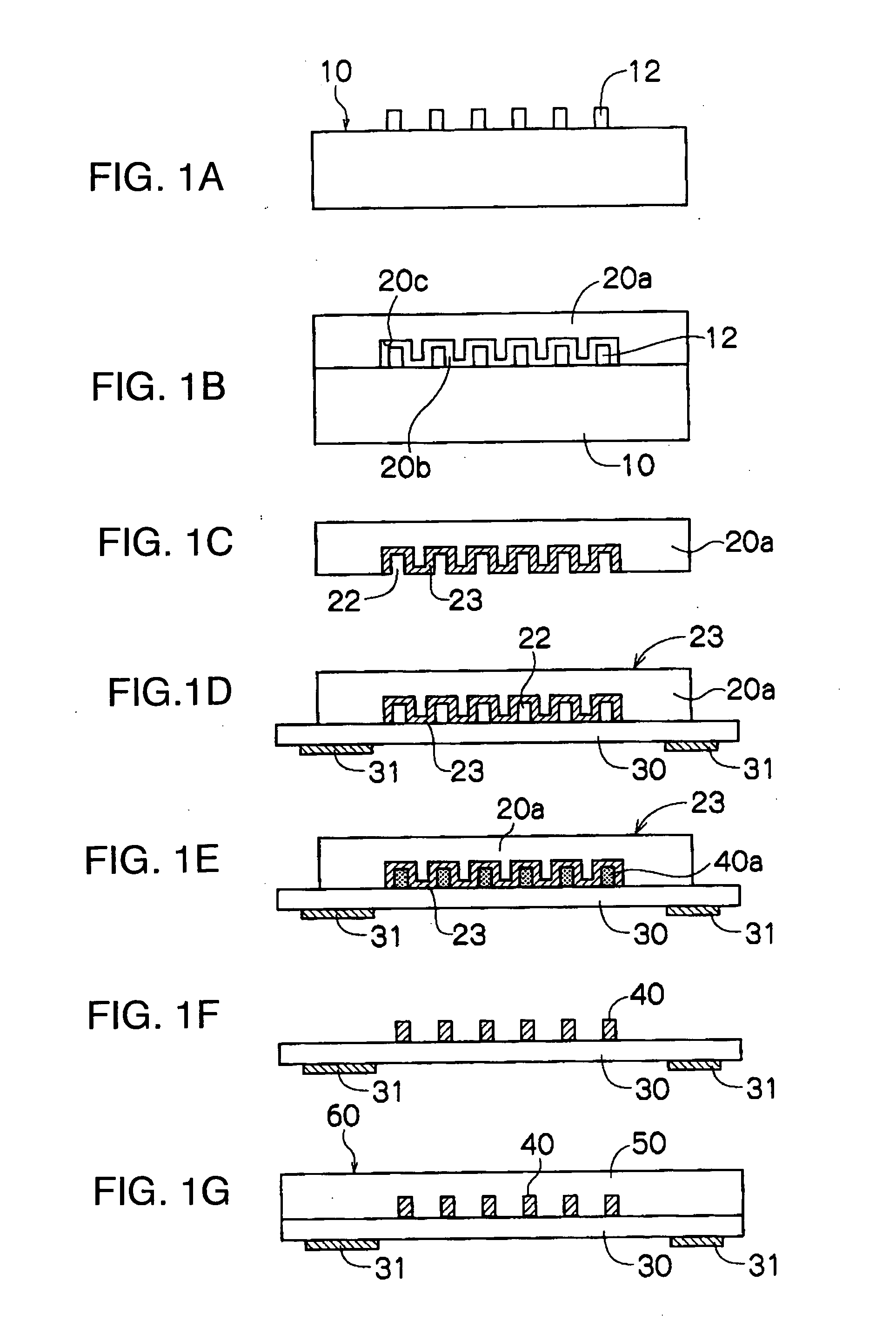
[0138] A UV-curable type thick film resist (manufactured by Microchemical Corp., with a trade name SU-8) is applied on a quartz substrate by a spin coat method, thereafter the coat on the quartz substrate is prebaked at 80° C., the resist is exposed to light by a high-pressure mercury light through a photomask, the exposed resist is developed to form five convex portions with a section in the shape of a square (50 μm in width, 50 μm in height, 500 μm in pitch and 50 mm in length). Then, the convex portion is post baked at 120° C. to form a core master template.

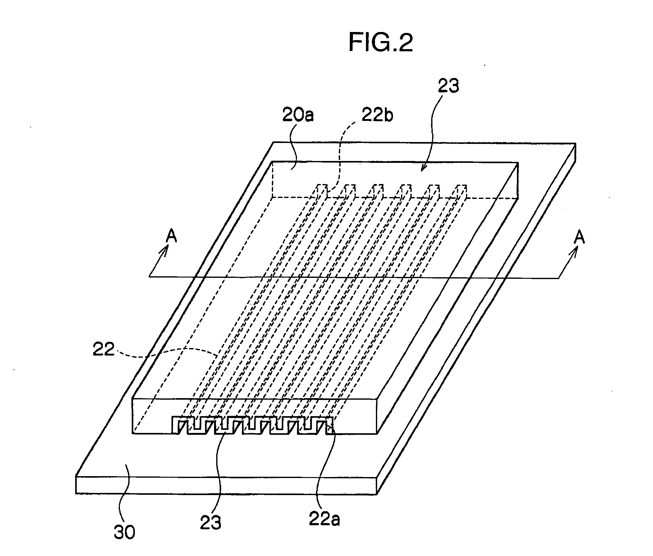
[0139] Then, a reinforced member (the thickness of 1.5 mm, and made of aluminum) in which the opening corresponding to a UV-irradiation part is formed and which has three inlets and three outlets is prepared. The rubber layer-forming concave portion including groove parts which (100 μm in width, 100 μm in height, 500 μm in pitch and 50 mm in length, five) are formed in the same pitch as...

Example

Comparative Example 1

[0147] The Arton film and the rubber mold made of a uniform rubber material having the Share rubber hardness of 80 are used, and an optical waveguide core and a cladding layer are formed in the same manner as in Example 1. Then the electric circuit is formed on the core non-forming surface of the Arton film in the same manner as in Example 1 to produce a polymer optical waveguide. The average wave guiding loss of three optical waveguide cores of the polymer optical waveguide is 5.3 dB / cm. Other two optical waveguide cores can not be confirmed. The shape deterioration of the optical waveguide core in the photolithography process in the formation of the electroconductive pattern of the electric circuit can be confirmed by a microscope.

Example

Example 2

Preparation of Rubber Mold

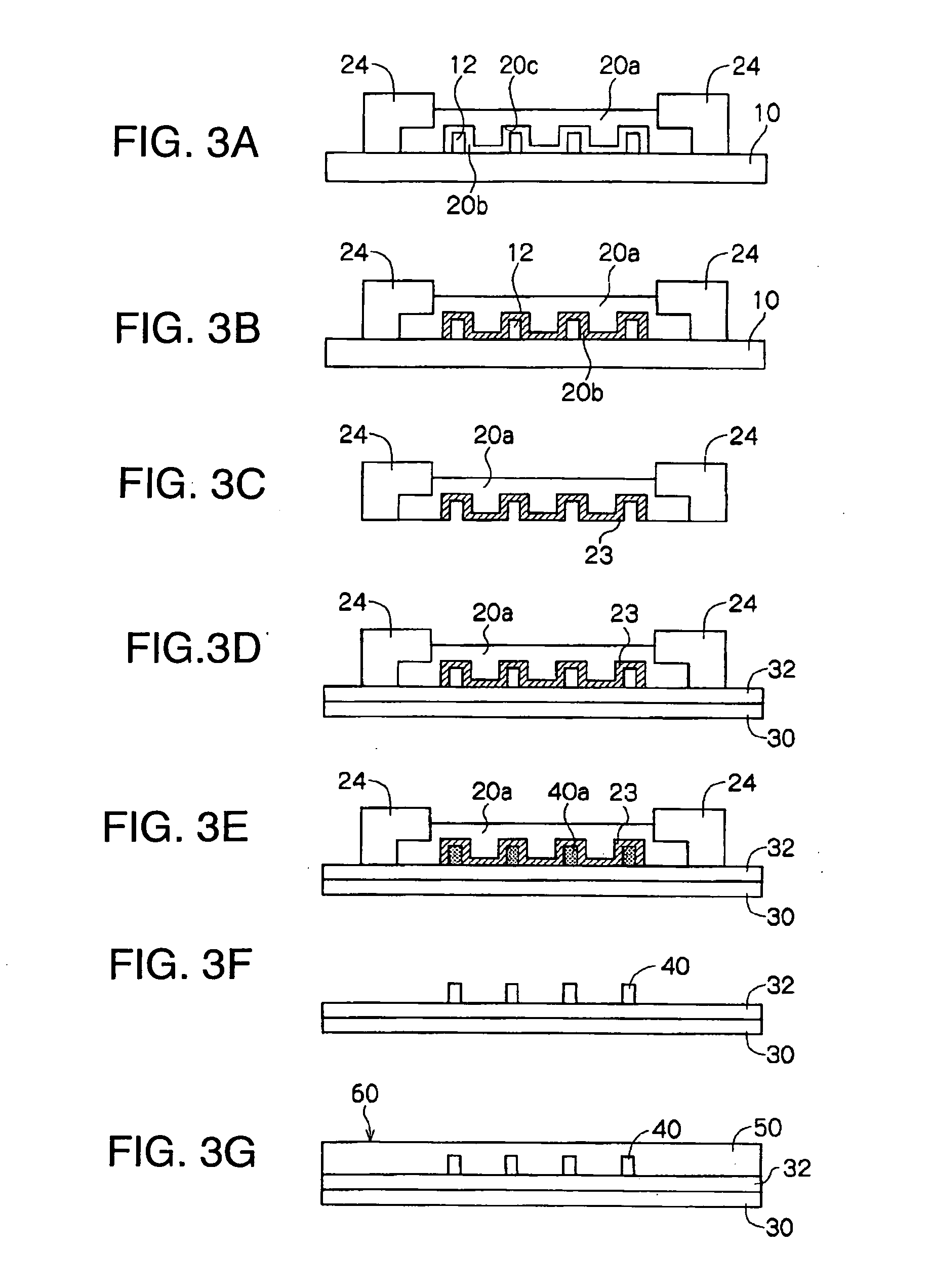
[0148] A UV-curable type thick film resist liquid (manufactured by Microchemical Corp., with a trade name SU-8) is applied on a silicon wafer substrate by a spin coat method, thereafter the coat on the silicon wafer substrate is prebaked at 80° C., the resist is exposed to light by a high-pressure mercury light through a photomask, the exposed resist is developed to form ten minute convex portions with a section in the shape of a square (100 μm in width, 100 μm in height, 1 mm in pitch and 100 mm in length). Then, the convex portion is post baked at 120° C. A pressure easing gap producing convex portion is formed on the edge part of the convex portion of the convex portions produced thus by the mold respectively. A pressure easing gap producing convex portion has the section of 2 mm in height, 10 mm in width (a direction that is orthogonal to the convex portion), and 20 mm in length of the longitudinal direction of a substrate and of a rectangle...


PUM

PropertyMeasurementUnit
Thicknessaaaaaaaaaa
Thicknessaaaaaaaaaa
Thicknessaaaaaaaaaa

Abstract

A process for producing a polymer optical waveguide including: 1) preparing a rubber mold having a composite layer structure in which a rubber layer which has a concave portion corresponding to an optical waveguide core and contains a rubber mold-forming curable resin is buried in a rubber layer-forming concave portion of a rigid substrate having the rubber layer-forming concave portion; 2) bringing a cladding substrate into close contact with the rubber mold; 3) filling the concave portion of the rubber mold, with which the cladding substrate has been brought into close contact, with a core-forming curable resin; 4) curing the filled core-forming curable resin; 5) removing the rubber mold from the cladding substrate; and 6) forming a cladding layer on the cladding substrate on which the core has been formed.

Description

[0001] This application claims priority under 35 USC 119 from Japanese Patent Application No. 2003-422136, the disclosure of which is incorporated by reference herein. BACKGROUND OF THE INVENTION [0002] 1. Field of the Invention [0003] The present invention relates to a process for producing a polymer optical waveguide, and particularly, to a process for producing a polymer optical waveguide by which a polymer optical waveguide can be formed on an embedded silicon substrate or an electric circuit substrate. [0004] 2. Description of the Related Art [0005] As a process for producing a polymer optical waveguide, the following processes are suggested: (1) a process of impregnating a film with a monomer, selectively exposing a core portion to light to change a refraction index thereof, and sticking a film thereto (selective polymerization); (2) a process of applying a core layer and a clad layer to a substrate, and forming a clad portion by reactive ion etching (RIE); (3) a process using...

Claims


Application Information

Patent Timeline
IPC IPC(8): B29C33/40G02B6/13B29C39/02B29C39/42B29D11/00G02B6/122
CPCB29C33/405B29C39/026G02B6/1221B29D11/00663B29C39/42Y10S977/877B29C37/005B29C35/0805B29C2035/0827B29C35/0888
Inventor AKUTSU, EIICHIOHTSU, SHIGEMISHIMIZU, KEISHIYATSUDA, KAZUTOSHI
Owner FUJIFILM BUSINESS INNOVATION CORP
Why Eureka
Try Eureka