Selective passivation of exposed silicon

a technology of exposed silicon and selective passivation, which is applied in the direction of liquid/solution decomposition chemical coating, transportation and packaging, coatings, etc., can solve the problems of high manpower cost and complex equipment, and achieve the effect of easy control of thickness and high manpower cos

Inactive Publication Date: 2005-07-28
MICRON TECH INC
View PDF23 Cites 54 Cited by
  • Summary
  • Abstract
  • Description
  • Claims
  • Application Information

AI Technical Summary

Benefits of technology

[0020] The present invention is a method for selectively forming a dense layer of passivating oxide, e.g., silicon dioxide or zirconium oxide, onto an exposed semiconductor wafer surface, e.g., silicon or germanium. The layer is applied by submersion of the exposed semiconductor wafer surface in a liquid at low or ambient temperature. The passivation layer of easily controlled thickness may be formed in a limited amount of time. The method differs from conventional high-temperature thermal oxidation, chemical vapor deposition, and spin-on passivation methods, each of which requires sophisticated equipment and high manpower costs. The method does not require inversion of a semiconductor wafer such as required by prior art back side deposition using spin-on deposition, nor does it require protracted heating at a high temperature to cure the layer.
[0021] The present invention is directed to the application of a silicon dioxide layer on an exposed silicon layer. The deposition is selective to silicon / silicon dioxide and may be performed by exposure to a liquid phase composition in a bath at room temperature or a temperature somewhat above room temperature, e.g., up to about 50° C. The liquid phase composition is supersaturated in silicon dioxide. The silicon dioxide deposition rate is not self-limiting, that is, it does not depend upon the layer thickness. The deposition rate may be readily controlled to provide repeatedly uniform layer thickness. Thus, for example, the method may be used to passivate the back side of a wafer or other semiconductor substrate without inverting the wafer or substrate. The method is specific to the base substrate, e.g., silicon and its oxide. Further exclusion of oxide from other surfaces may be assured by, for example, covering such surfaces with tape. Any silicon dioxide pre-existing on the silicon surface may be first removed or, alternatively, left in place for oxide deposit thereover.
[0023] The exposed copper or aluminum metallization at each bond pad location may then be coated with immersion palladium or zinc, followed by an electroless nickel and, optionally, immersion gold, in a bath to form pads amenable to soldering or another joint with an external conductor. For example, the bond pads may then be coated with gold or solder-bonded to conductive wires. The overall process results in devices which are produced at reduced time and expense and which are more reliable than those currently produced.

Problems solved by technology

The method differs from conventional high-temperature thermal oxidation, chemical vapor deposition, and spin-on passivation methods, each of which requires sophisticated equipment and high manpower costs.

Method used


Image

  • Selective passivation of exposed silicon
  • Selective passivation of exposed silicon
  • Selective passivation of exposed silicon

Examples


Embodiment Construction

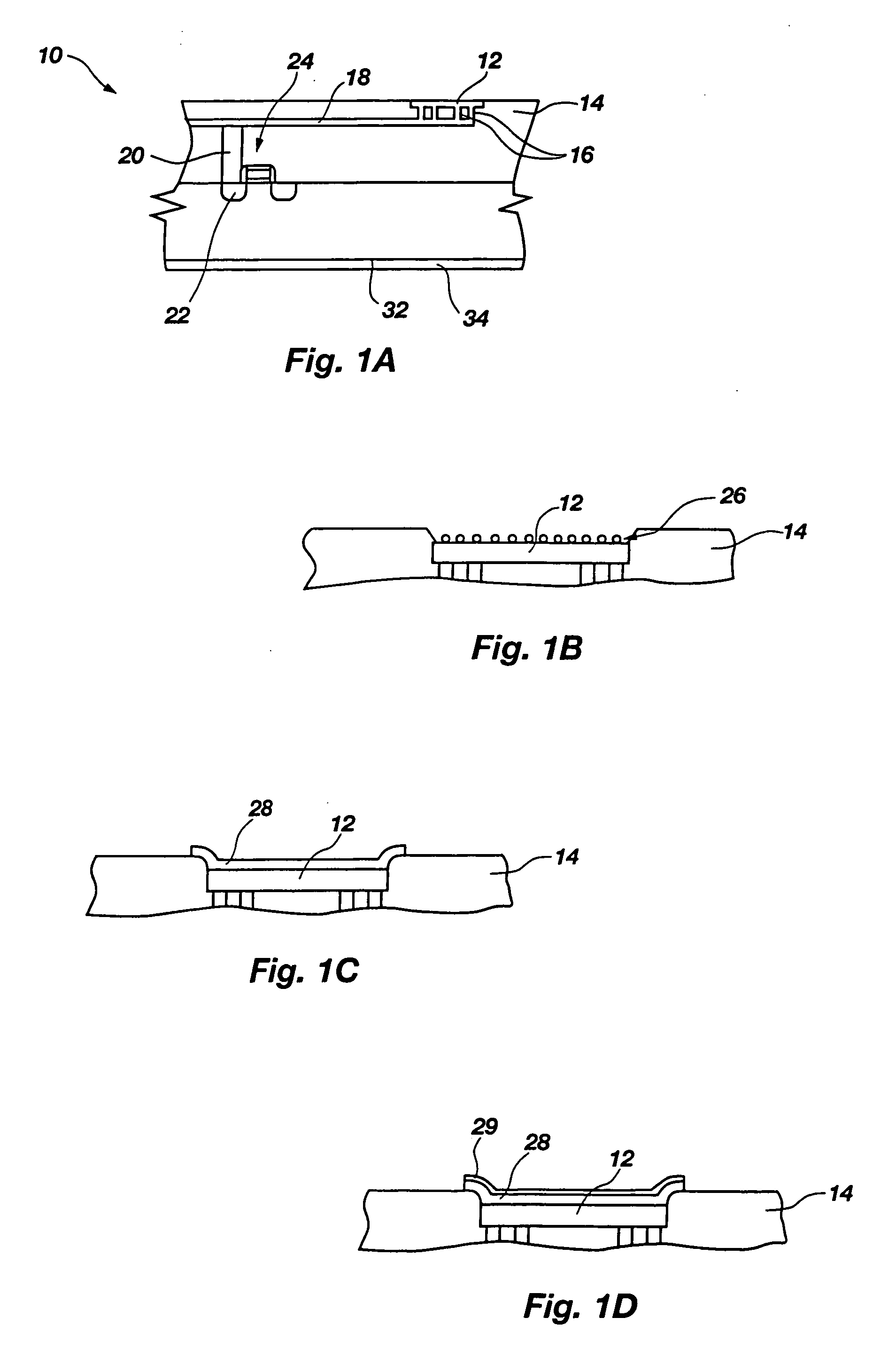
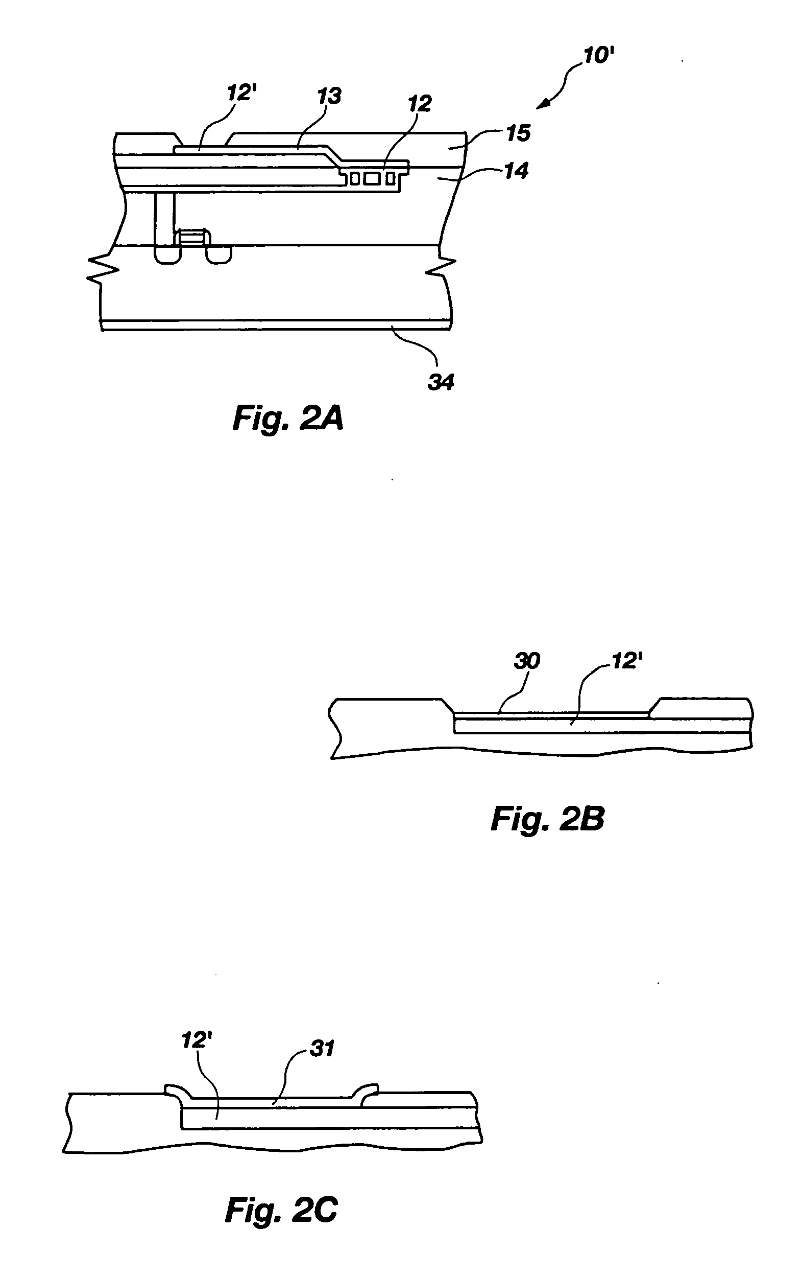
[0033] With reference to FIGS. 1A-1D and 2A-2C, different types of bond pads 12, 12′ that are typically used in semiconductor devices 10, 10′ are depicted. In FIG. 1A, a semiconductor device which includes copper bond pads 12 is shown. Copper bond pads 12 are typically formed on a passivation layer 14 of semiconductor device 10 and communicate with underlying, integrated circuitry of semiconductor device 10. By way of example, one or more generally downwardly extending conductive vias 16 may establish electrical communication with conductive traces 18, or “runners,” that, in turn, electrically communicate with the integrated circuitry of semiconductor device 10. For example, runners 18 may lead to contact plugs 20 that provide a conductive link between runners 18 and a conductively doped silicon active-device region 22 of a transistor 24 of semiconductor device 10.

[0034] In order to use a rapid electroless plating method to plate bond pads 12, 12′ without incurring damage to the se...


PUM

PropertyMeasurementUnit
temperatureaaaaaaaaaa

Abstract

A method for applying a passivation layer selectively on an exposed silicon surface from a liquid phase solution supersaturated in silicon dioxide. The immersion is conducted at substantially atmospheric temperature and pressure and achieves an effective passivation layer in an abbreviated immersion time, and without subsequent heat treatment. In one embodiment, rapid coating of a wafer back side with silicon dioxide permits the use of a high-speed electroless process for plating the bond pad with a solder-enhancing material. In another embodiment, the walls of via holes and microvia holes in a silicon body may be passivated by immersion in the supersaturated solution prior to plugging the holes with conductive material.

Description

CROSS-REFERENCE TO RELATED APPLICATIONS [0001] This application is a continuation of application Ser. No. 10 / 454,254, filed Jun. 3, 2003, pending, which is a continuation of application Ser. No. 10 / 218,268, filed Aug. 13, 2002, now U.S. Pat. No. 6,593,221, issued Jul. 15, 2003.BACKGROUND OF THE INVENTION [0002] 1. Field of the Invention [0003] The present invention relates to methods for electrically isolating dielectric materials. More particularly, the invention pertains to methods for electrical isolation, i.e., passivation of exposed silicon such as occurs on the back side of a semiconductor (SC) wafer comprising semiconductor devices or dice of a DRAM, SRAM, or other semiconductor die configuration. The invention also pertains to passivation of apparatus such as carrier substrates, interposer substrates for flip-chip packaging, conductive interconnects for test packages, and the like. [0004] 2. Background of Related Art [0005] Silicon is a basic material from which a broad rang...

Claims


Application Information

Patent Timeline
Patent Type & Authority Applications(United States)
IPC IPC(8): H01L21/288H01L21/316H01L21/60H01L23/485H01L23/522
CPCC23C18/1208Y10T428/12854H01L21/02282H01L21/288H01L21/316H01L21/31612H01L23/3171H01L23/5226H01L24/11H01L27/105H01L2224/05082H01L2224/05147H01L2224/05155H01L2224/05644H01L2224/05655H01L2224/13099H01L2924/01005H01L2924/01006H01L2924/01013H01L2924/01014H01L2924/01022H01L2924/01028H01L2924/01029H01L2924/0103H01L2924/01032H01L2924/0104H01L2924/01046H01L2924/01074H01L2924/01078H01L2924/01079H01L2924/01082H01L2924/014H01L2924/14H01L21/02164H01L2224/0401H01L2924/01072H01L2924/01033H01L24/05H01L2924/01021H01L2924/01023H01L2924/00014H01L2924/12042H01L2924/00
Inventor LINDGREN, JOSEPH T.
Owner MICRON TECH INC
Why Eureka
Try Eureka