Process and apparatus for removing residues from semiconductor substrates

Inactive Publication Date: 2005-08-25
BATTELLE MEMORIAL INST
View PDF54 Cites 57 Cited by
  • Summary
  • Abstract
  • Description
  • Claims
  • Application Information

AI Technical Summary

Benefits of technology

[0007] The reactive systems of the present invention are distinguished from other densified fluid cleaning systems known in the art in at least the following key areas. First, the present invention embodies reactive approaches for effecting residue removal and / or cleaning that are viable and applicable to commercial wafer and / or semiconductor processing. Test results show, for example, that residue removal is effected to industry accepted contamination standards or better. One such measure for commercial processing is the atomic monolayer standard for residue per unit area. For example, a monolayer of pure silicon on a wafer surface may be calculated to comprise a coverage of approximately 2×10¹⁵ atoms per square centimeter (e.g., atoms / cm2). The systems of the present invention have been shown to remove residues to a level of about 4×10¹¹ atoms / cm2 or better, making them ultimately viable for commercial use. Secondly, systems of the present invention offer enhanced speeds and / or efficiencies for effecting removal of residues. For example, residue removal occurs in a maximum period up to 15 minutes. Typical periods for residue removal occur in 5 minutes or less on average. Periods of 15 seconds are presently ideal. Thirdly, and significantly, the systems embodied in the present invention exert low surface tension stresses on small wafer features, thus being ultimately useful for commercial processing applications into the next generation of feature development and beyond.
[0022] Effectiveness of a reactive cleaning system for wafer or semiconductor processing is also a function of 1) maintaining a sufficiently low surface tension to minimize damage to the critical or intricate surface structures; 2) retaining dimensional and / or site attributes of the patterned features or structures of a substrate or wafer surface during processing; 3) retaining a sufficient polarity in the cleaning fluid for solubility among and between the various chemical moieties, modifiers, and constituents; and 4) maintaining reactivity between and among the chemically reactive modifiers and / or constituents in the densified fluid medium so as to effect residue removal.
[0024] It is an object of the present invention to show a reactive reverse-micelle cleaning system that 1) optimizes wafer cleaning performance by removing etch residues and other metal and non-metal residues; 2) comprises low quantities of chemical modifiers; and 3) exhibits low overall toxicity. The term “modifiers” defines any additive (chemical or otherwise) introduced to the fluids of the present systems to enhance reactivity, cleaning performance, speed, and / or efficiency for removing tenacious residues. Preference is given to modifiers, additives, solvents, and fluids that in the various application aspects are easily recovered and that lower commercial processing costs. Optimization benchmarks include achieving 1) essentially complete removal of residues; 2) greater efficiency and / or speed of residue cleaning than is currently known in the art; 3) cleaning levels for residues that remain efficacious for commercial wafer and / or semiconductor processing; and 4) a reduction in the number of critical dimension (CD) changes to substrate features and patterns (e.g., vias) or other important substrate structures. The term “critical dimension” changes refers to alterations in the size or dimensions (e.g., pitch) of patterns or structural features such as vias on the wafer substrate or surface. Preference is given to systems that minimize changes to functional components of the wafer surface or substrate.

Problems solved by technology

Electrical components of semiconductor devices are now approaching sizes and / or dimensions such that surface tension generated by conventional aqueous and semi-aqueous cleaning solutions during manufacturing may damage the extremely delicate electrical components and / or features.
Ultimately the surface tension exerted in these liquids on the small wafer surface features and patterns will exceed the critical stress, the point of structural failure, making conventional aqueous and semi-aqueous fluids unsuitable or at worst obsolete for next-generation processing and cleaning of substrates, wafers, and / or semiconductors.
Presence of such residues following processing may lead to a faulty or failed device.
However, a major drawback of densified fluid systems is that they are non-reactive, having no ability to directly chemically modify and remove tenacious metal and non-metal residues generated during wafer processing.

Method used


Image

  • Process and apparatus for removing residues from semiconductor substrates
  • Process and apparatus for removing residues from semiconductor substrates
  • Process and apparatus for removing residues from semiconductor substrates

Examples


example 1

Reverse Micelle System Comprising Perfluoropolyether Phosphate Surfactant / Alkyl Sulfonate Co-Surfactant / Water

Residue Cleaning System

[0061]FIG. 6 illustrates a reactive reverse micelle(s) system according to a first embodiment of the present invention. Illustrated is a perfluoro-poly-ether (PFPE) phosphate surfactant / alkyl-sulfonate (AOT) co-surfactant / water system for removing etch residues 650 and non-metal residues 650 found to be tenacious and problematic residues for semiconductor and / or wafer substrate surface processing. This system has very attractive attributes for commercial processing including very low quantities of modifiers, very low volatility, ease of fluid recovery, low toxicity, minimal CD changes, and high speed cleaning. Cleaning occurs preferably in a time below about 15 minutes per wafer on average, and more preferably in less than about 5 minutes.

[0062] The system of the present embodiment comprises reactive reverse micelles 620 or reactive aggregates 620 co...

example 2

Reverse Micelle System Comprising Perfluoropolyether Ammonium Carboxylate Surfactant / Hydroxylamine / Water

Residue Cleaning System

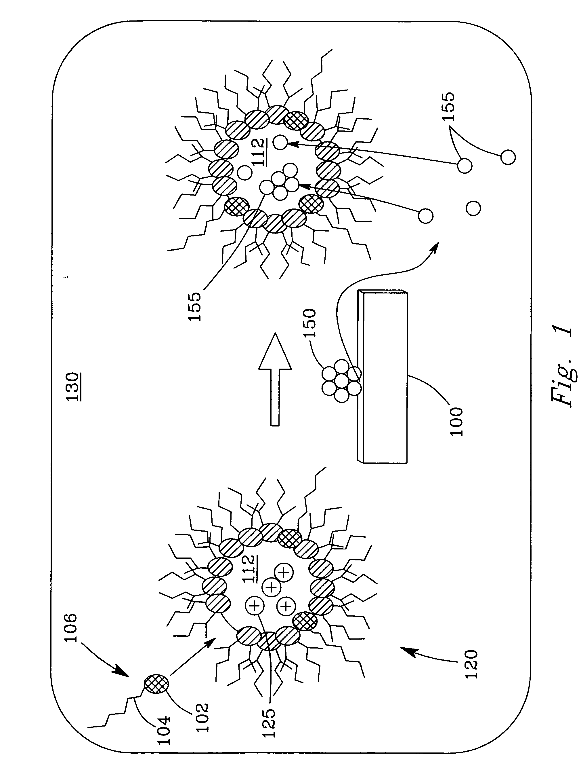
[0066]FIG. 8 illustrates a reactive micelle system according to a second embodiment of the present invention. Illustrated is a PFPE-ammonium carboxylate / hydroxylamine system for removing etch and non-metal residues 850 found to be tenacious and problematic residues for semiconductor substrate and wafer surface processing.

[0067] The system of the instant embodiment comprises reactive reverse micelles 820 or reactive macro-molecular aggregates 820 comprising a fluorinated reverse micelle-forming surfactant, perfluoro-poly-ether (PFPE) ammonium carboxylate 806, in a densified CO2 phase 830. The surfactant 806 comprises a carboxylate headgroup 802 and a perfluoro-poly-ether (PFPE) tail 804. The carboxylate headgroups 802 align in close proximity to surround and form the inner polar core 814 of the aggregate 820. The PFPE tail 804 provides solubility in the de...

example 3

Reverse Micelle System Comprising Fluorocarbon Phosphate Acid Surfactant / Alkyl Sulfonate Co-Surfactant / Benzotriazole (BTA) / Water

Metal Residue Cleaning System

[0075] In a third embodiment of the present invention, a surfactant / co-surfactant / corrosion inhibitor / water system has been shown to be effective for removing metal residues (e.g., Cu, Fe, Al, etc.) found to be tenacious and problematic residues for semiconductor (e.g., silicon) substrate and wafer surface processing. The instant system has very attractive attributes for commercial processing including very low quantities of modifiers, very low volatility, ease of fluid recovery, low toxicity, minimal CD changes, and high speed cleaning (less than about 5 minutes per wafer on average).

[0076] Testing was conducted on a porous low-K dielectric (LKD) “barrier-open” (BO) wafer coupon 600 (e.g., LKD BO) having significant levels of copper residue 650. The system of the present embodiment is composed of reactive reverse micelle(s) ...


PUM

PropertyMeasurementUnit
Temperatureaaaaaaaaaa
Fractionaaaaaaaaaa

Abstract

The present invention generally relates to a system for cleaning substrates. More particularly, the present invention relates to process(es) for effecting chemical removal of residues from semiconductor substrates, including silicon wafers, using a system of reactive reverse micelle(s) or microemulsions in a densified carbon dioxide matrix. Various reactive chemical agents in the reactive micelle system may be used to effect cleaning and removal of etch and metal residues to levels sufficient for commercial wafer production and processing.

Description

FIELD OF THE INVENTION [0001] The present invention generally relates to a process and apparatus for cleaning substrates. More particularly, the present invention relates to processes for removing residues including etch, metal, and non-metal residues from semiconductor substrates. The instant invention finds application in many processes such as commercial silicon wafer production. BACKGROUND [0002] The semiconductor industry faces challenges to produce devices with increasingly smaller features to increase electrical component density per unit area on a wafer and to enhance operating speed of the semiconductor. Electrical components of semiconductor devices are now approaching sizes and / or dimensions such that surface tension generated by conventional aqueous and semi-aqueous cleaning solutions during manufacturing may damage the extremely delicate electrical components and / or features. Ultimately the surface tension exerted in these liquids on the small wafer surface features and...

Claims


Application Information

Patent Timeline
IPC IPC(8): B08B7/00C11D1/12C11D1/14C11D1/34C11D11/00H01L21/02H01L21/306H01L21/311H01L21/768
CPCB08B7/0021C11D1/123C11D1/146H01L21/76814C11D11/0047H01L21/02063H01L21/02101C11D1/345C11D2111/22H01L21/304
Inventor FULTON, JOHN L.GASPAR, DANIEL J.YONKER, CLEMENT R.YOUNG, JAMES S.LEA, ALAN SCOTTENGELHARD, MARK H.
Owner BATTELLE MEMORIAL INST
Why Eureka
Try Eureka