Method for manufacturing thin film transistor

a thin film transistor and manufacturing method technology, applied in the direction of crystal growth process, polycrystalline material growth, chemistry apparatus and processes, etc., can solve the problem of imposing a substantial processing burden on the circuit design

Inactive Publication Date: 2005-09-01
VISTA PEAK VENTURES LLC
View PDF16 Cites 4 Cited by
  • Summary
  • Abstract
  • Description
  • Claims
  • Application Information

AI Technical Summary

Benefits of technology

[0007] An object of the present invention is to provide a method for manufacturing a thin film transistor that constitutes p-channel and n-channel transistors exhibiting smaller span of variations in threshold voltage levels.

Problems solved by technology

Accordingly, it can be concluded that although a P-channel transistor is formed to have threshold voltage levels within a specific range of values, a P-channel transistor and an N-channel transistor are formed to have threshold voltages at levels different from each other due to the variation of N-channel transistor threshold voltage, incurring a substantial processing burden on the design of circuit.

Method used


Image

  • Method for manufacturing thin film transistor
  • Method for manufacturing thin film transistor
  • Method for manufacturing thin film transistor

Examples


first embodiment

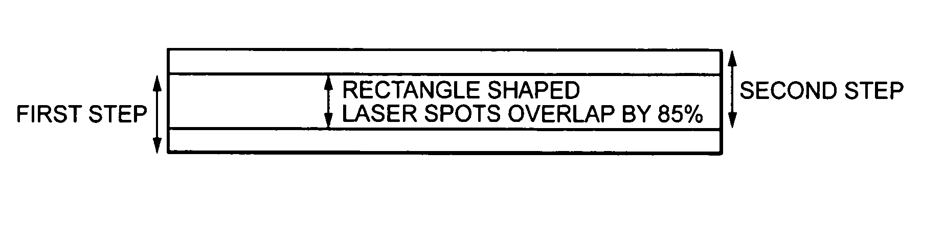
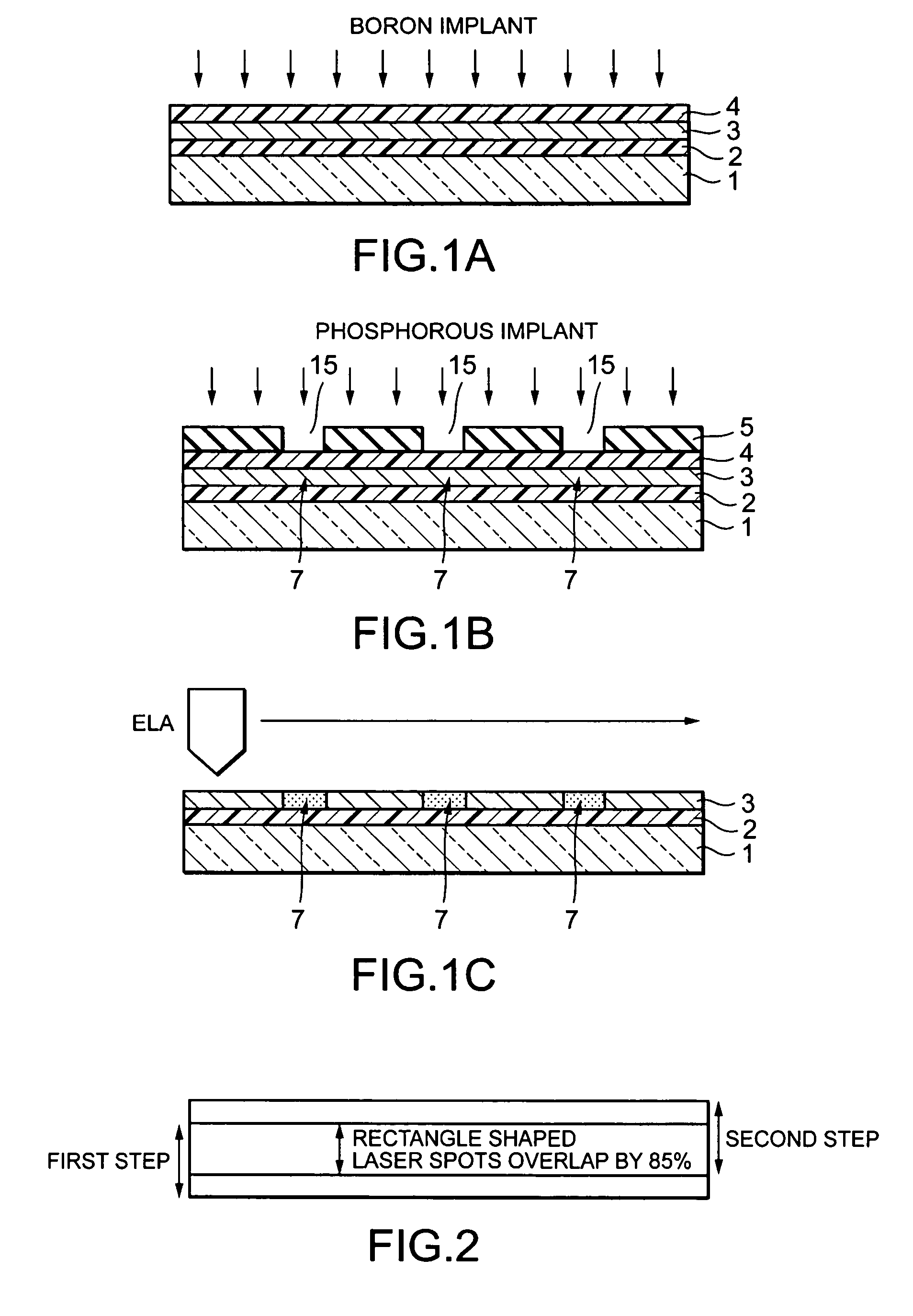
[0018] A method for manufacturing a thin film transistor according to the invention will be explained in detail below. FIGS. 1A, 1B and 1C are cross sectional side views of a TFT substrate constituting a liquid crystal panel and illustrate a part of process steps of a method for forming a thin film transistor on a transparent insulating substrate, in the order of process steps. Furthermore, FIG. 2 is a plan view illustrating how the TFT substrate is subjected to a multi-step radiation process, in which rectangle-shaped Excimer laser radiation is used for manufacture of thin film transistor.

[0019] First, an amorphous silicon film 3 is deposited over a transparent insulating substrate 1 via an insulation film 2. Then, for example, a boron dopant is implanted into the entire amorphous silicon film 3 via the insulation film 4 to adjust the threshold voltage of an N-channel transistor (refer to FIG. 1A).

[0020] Thereafter, a resist film is coated over the amorphous silicon film 3 and exp...

second embodiment

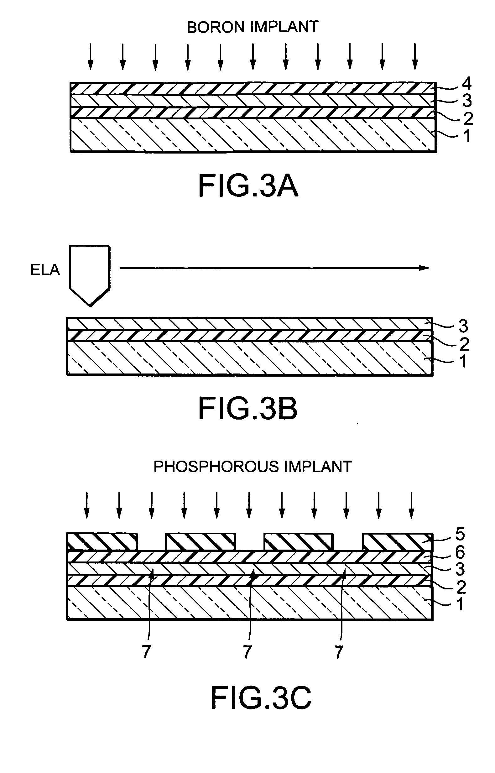
[0027] Subsequently, a method for manufacturing a thin film transistor according to the invention will be explained below.

[0028] The method according to the first embodiment includes implanting two dopant atoms of different conductivity types into the amorphous silicon film and converting the amorphous silicon of the amorphous silicon film into polycrystalline silicon through the use of Excimer laser. That is, boron ions are implanted into the amorphous silicon film within the N-channel transistor formation region and both boron and phosphorous ions are implanted into the amorphous silicon film within the P-channel transistor formation region. However, employment of a method including implanting one dopant into the amorphous silicon film and then converting the amorphous silicon of the amorphous silicon film into polycrystalline silicon through the use of Excimer laser produces beneficial effects similar to those resulting from employment of the method according to the first embodim...

third embodiment

[0035] According to the method employed in the third embodiment, in addition to converting the amorphous silicon of amorphous silicon film into polycrystalline silicon, the dopant atoms doped into the amorphous silicon film act to terminate dangling bonds that occur at surfaces and interfaces in the amorphous silicon film and therefore, localized levels caused by the dangling bonds that occur at surfaces and interfaces in the amorphous silicon film 3 are reduced. This allows standard deviation (σ) of variations in threshold voltages of N-channel and P-channel transistors to significantly be reduced from 0.18 V to 0.09 V and from 0.25 V to 0.09 V, respectively.

[0036] When heating the amorphous silicon to temperatures below 290 degrees C., solid phase diffusion rarely occurs, i.e., the extent to which variations in the threshold voltages of N-channel and P-channel transistors are reduced becomes small and when heating the amorphous silicon to temperatures not greater than 350 degrees ...


PUM

PropertyMeasurementUnit
thicknessaaaaaaaaaa
thicknessaaaaaaaaaa
thicknessaaaaaaaaaa

Abstract

Prior to converting a non-single crystal material of a semiconductor film into a single crystal material through the use of a laser beam, at least one dopant is introduced into whole of the semiconductor film. Then, the non-single crystal semiconductor film is irradiated with a laser beam to crystallize the semiconductor film. In this case, a ratio between quasi-fermi level of the single crystal material within one of transistor formation regions used to form transistors of different conductivity types and quasi-fermi level of the single crystal material within the other thereof is made to be between 0.5:1 and 2.0:1. Thus, transistors of different conductivity types are formed in the crystallized semiconductor film.

Description

CROSS-REFERENCE TO RELATED PATENT APPLICATIONS [0001] This application is a continuation of application Ser. No. 10 / 617,170, filed Jul. 11, 2003, now pending, and based on Japanese Patent Application No. 2002-211500, filed Jul. 19, 2002, by Mitsuasa Takahashi. This application claims only subject matter disclosed in the parent application and therefore presents no new matter.BACKGROUND OF THE INVENTION [0002] 1. Field of the Invention [0003] The present invention relates to a method for manufacturing p-type and n-type thin film transistors, and particularly to a method for manufacturing a thin film transistor through a laser radiation process. [0004] 2. Description of the Related Art [0005] Conventionally, there are two primary methods for irradiating amorphous silicon with an Excimer laser (EL) beam to anneal the amorphous silicon, converting the amorphous silicon into polycrystalline silicon. One of the two primary methods includes converting amorphous silicon into polycrystalline...

Claims


Application Information

Patent Timeline
Patent Type & Authority Applications(United States)
IPC IPC(8): C30B1/00H01L21/20H01L21/268H01L21/336H01L21/77H01L21/84H01L27/12H01L29/786
CPCC30B1/00H01L21/2026H01L21/268H01L27/1285H01L27/12C30B29/06H01L29/786H01L21/02675
Inventor TAKAHASHI, MITSUASA
Owner VISTA PEAK VENTURES LLC
Why Eureka
Try Eureka