Photoelectric conversion film, photoelectric conversion element, imaging element, method of applying electric field thereto and electric field-applied element

a technology of photoelectric conversion and imaging element, applied in the direction of solid-state devices, semiconductor devices, radio frequency controlled devices, etc., can solve the problems that the proposals in these documents are hardly applicable to photoconductive films, and the size and weight of such imaging devices of the three-sheet structure are unavoidable, and achieve excellent color reproduction, high photoelectric conversion efficiency, and excellent durability.

Active Publication Date: 2005-09-22
FUJIFILM HLDG CORP +1
View PDF7 Cites 96 Cited by
  • Summary
  • Abstract
  • Description
  • Claims
  • Application Information

AI Technical Summary

Benefits of technology

[0069] The photoelectric conversion film, photoelectric conversion element and imaging element according to the invention are each advantageous in having a narrow half bandwidth of absorption, showing excellent color reproduction, showing a high photoelectric conversion efficiency and being excellent in durability. In two-layered solid-state imaging elements and BRG three-layered solid-state imaging elements, in addition thereto, the following characteristics are established.
[0070] Due to the laminated structure, there arises no moire and, therefore, it is unnecessary to use an optical low pass filter. As a result, a high resolution can be achieved without color spreading. Moreover, signal processing can be easily c

Problems solved by technology

However, it is unavoidable that such an imaging device of the three sheet-structure has a large size and a large we

Method used


Image

  • Photoelectric conversion film, photoelectric conversion element, imaging element, method of applying electric field thereto and electric field-applied element
  • Photoelectric conversion film, photoelectric conversion element, imaging element, method of applying electric field thereto and electric field-applied element
  • Photoelectric conversion film, photoelectric conversion element, imaging element, method of applying electric field thereto and electric field-applied element

Examples


example 1

[0294] On an indium tin oxide (hereinafter referred to as ITO) film, a layer (film thickness: 50 nm) of 1,3 -diphenyl-5-[(3 -(2-phenoxyethyl)-2(3H)-5-phenylbenzoxazolidene)ethyldene]ethylidene]-2-,4,6-(1H,3H,5H)-pyrimidintrione (dimethine merocyanine: Compound 1) was formed by the vacuum vapor deposition method. Next, a layer (film thickness: 50 nm) of perylene-3,4,9,10-tetracarboxyl-bis-benzimidazole (Compound 2) was formed. Further, a translucent aluminum electrode (film thickness: 40 nm) was formed to give a photoconductive film A. A photoconductive film B having a copper phthalocyanine (Compound 3) layer (film thickness: 50 nm) and a layer of (Compound 2) (film thickness: 50 nm) was employed for comparison.

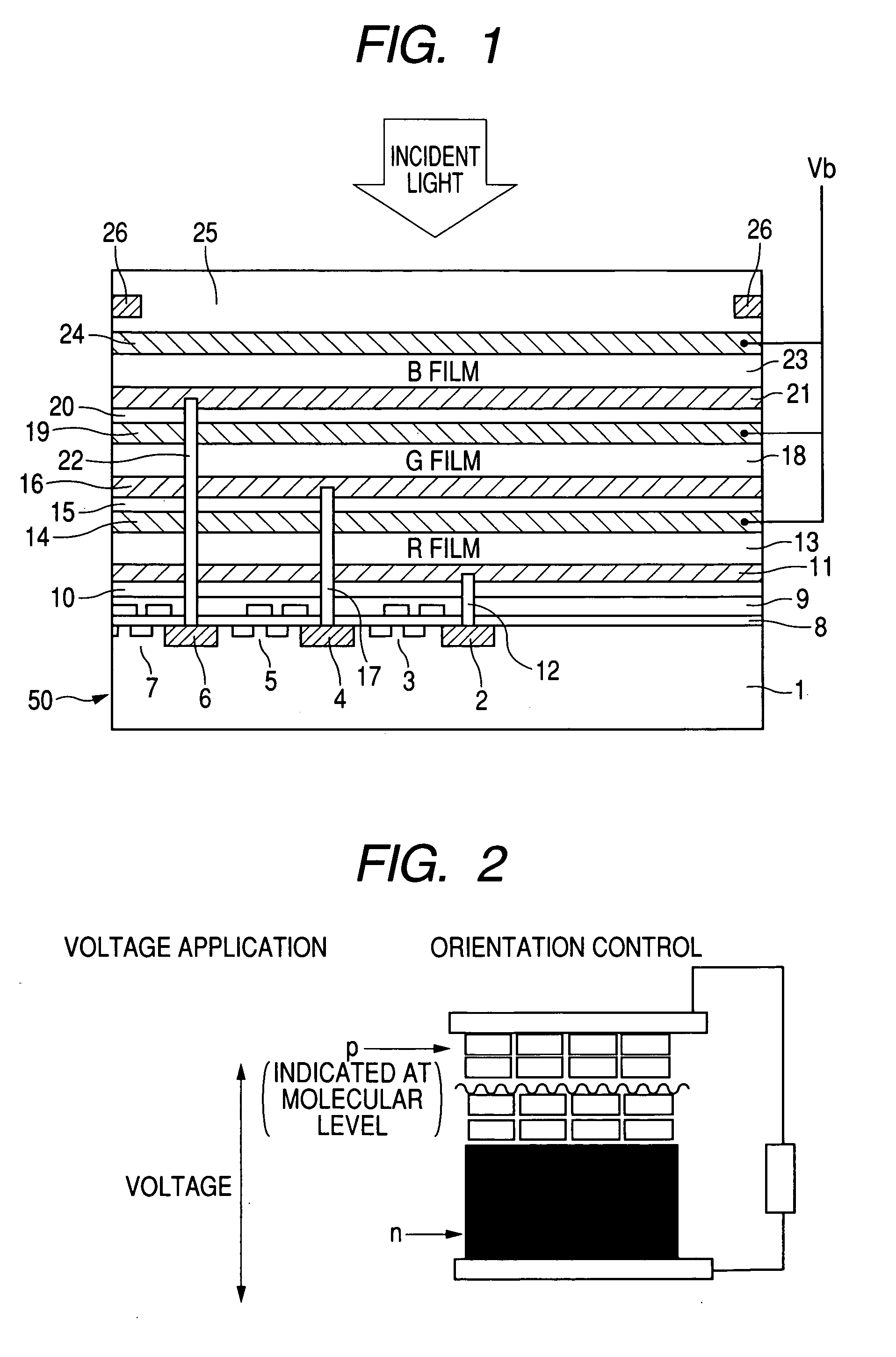
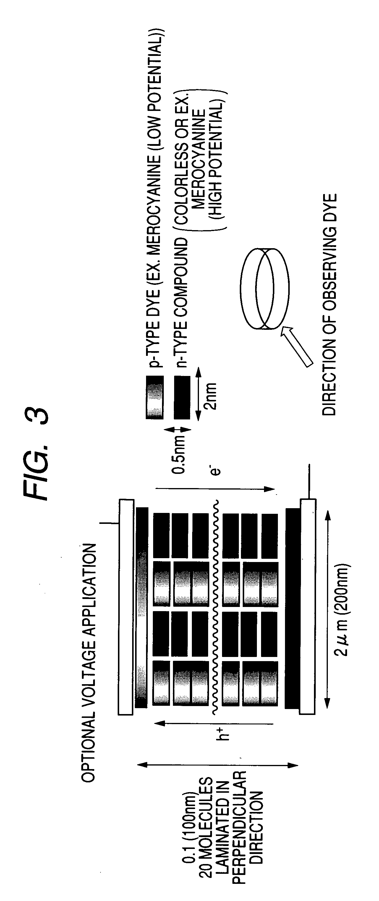
[0295] By analyzing the electron diffraction image of the photoconductive film A, it was clarified that (Compound 1) has an orientation as shown in the schematic diagram (FIG. 2). Since (Compound 1) has high self-aggregation properties, such a stable structure was formed. It ...

example 2

[0299] On an indium tin oxide (hereinafter referred to as ITO) film, a layer (film thickness: 10 nm) of 1,3-diphenyl-5-[(3-(2-phenoxyethyl)-2(3H)-5-phenylbenzoxazolidene)ethyldene]ethylidene]-2-,4,6-(1H,3H,5H)-pyrimidintrione (dimethine merocyanine: Compound 1) was formed by the vacuum vapor deposition method. Next, a layer (film thickness: 80 nm) was formed by simultaneous vapor deposition of (Compound 1) with 1,3-dicyanoethyl-5-[(3-benzyl-2(3H)-5-naphth[2,3-d]oxazolylidene]ethyldene]ethylidene]-2,4,6-(1H,3H,5H)-pyrimidintrione (dimethine merocyanine: Compound 4) at a ratio of 1:1. Next, a layer of (Compound 4) (film thickness: 10 nm) was formed by vapor deposition. Further, a translucent aluminum electrode (film thickness: 40 nm) was formed to give a photoconductive film C. The photoconductive film B as described in Example 1 was employed for comparison. By analyzing the electron diffraction image of the photoconductive film C, it was clarified that the compound has an orientation...

example 3

[0303] An element, which was produced as in Example 2 but substituting the compounds employed in the imaging element of Example 2 as follows, showed excellent performance similar to Example 2 compared with the comparison element.

[0304] (Compound 1) was substituted by tetramethine merocyanine (Compound 5) having four methine chains.

[0305] (Compound 4) was substituted by tetramethine merocyanine (Compound 6) having four methine chains.


PUM


Abstract

An imaging element having a photoelectric conversion film which has a laminated structure comprising a p-type semiconductor layer and an n-type semiconductor layer between a pair of electrodes, wherein at least one of the p-type semiconductor and the n-type semiconductor contains an organic compound with controlled orientation; a photoelectric conversion film having at least one organic dye compound, wherein the organic dye compound forms a J aggregate, or the angle between the spectral absorption transition dipolar moment of the organic dye compound and the photoelectric conversion film plane is 40° or less, a photoelectric conversion element and an imaging element; and a method of applying an electric field thereto, and an imaging element which comprises a photoelectric conversion film (a photosensitive layer) having a bulk heterojunction layer as an intermediate layer, or a photoelectric conversion film having two or more repeating structure units of a pn junction layer comprising a p-type semiconductor layer and an n-type semiconductor layer between a pair of electrodes.

Description

FIELD OF THE INVENTION [0001] This invention relates to a photoelectric conversion film, a photoelectric conversion element having this photoelectric conversion film and a solid-state imaging element, a method of applying an electric field thereto and an electric field-applied element. BACKGROUND OF THE INVENTION [0002] Photoelectric conversion films have been widely used in, for example, optical sensors. In particular, they are appropriately employed as solid-state imaging elements (photoreceptors) in imaging devices (solid-state imaging devices) such as TV cameras. Concerning materials of photoelectric conversion films to be used as solid-state imaging elements in imaging devices, films made of inorganic materials such as Si films and a-Se films are mainly employed. [0003] Conventional photoelectric conversion films with the use of these films made of inorganic materials have no sharp wavelength-dependency in the photoelectric conversion properties thereof In imaging devices with ...

Claims


Application Information

Patent Timeline
IPC IPC(8): H01L27/146H01L27/30H01L31/062H01L51/00H01L51/42
CPCH01L27/14647H01L27/307H01L51/0012Y02E10/549H01L51/007H01L51/424H01L51/4253H01L51/0064H10K39/32H10K71/191H10K85/652H10K85/6565H10K30/30H10K30/20
Inventor HIOKI, TAKANORI
Owner FUJIFILM HLDG CORP
Why Eureka
Try Eureka