Optical communication-use wavelength conversion device

a wavelength conversion device and communication technology, applied in the field of optical wavelength converters, can solve the problems of slow conversion speed, device requirement, disadvantageous integration and cost, etc., and achieve the effect of increasing the efficiency of wavelength conversion

Inactive Publication Date: 2005-09-29
NAT INST FOR MATERIALS SCI
View PDF4 Cites 6 Cited by
  • Summary
  • Abstract
  • Description
  • Claims
  • Application Information

AI Technical Summary

Benefits of technology

[0039] In this invention, since there is an invention for controlling the direction of polarization of the light that is input into the quasi-phase matched quartz crystal, the direction of polarization of the light can be adjusted to a direction that is desirable for the wavelength conversion of the quasi-phase matched quartz crystal by means of this control invention, so that the wavelength conversion efficiency can be increased.

Problems solved by technology

In such a method, however, the following problem arises: namely, the conversion speed is slow, and a conversion device is required for each wavelength.
Accordingly, this method is disadvantageous in terms of integration and cost.
In the case of this method, however, the following problem arises: namely, the wavelength conversion band is limited to the interior portion of the C band within the gain range of the semiconductor, so that inter-band wavelength conversion is impossible.
The possibility that the phase matching conditions will differ from place to place in such a long fiber is large, so that there are problems in terms of wavelength stability.
Moreover, the following problem also arises: namely, since the wavelength bandwidth that can be converted is inversely proportional to the length of the fiber, the conversion band is limited.
However, the following problems arise in a quasi-phase matching nonlinear optical element using a ferroelectric crystal.
Namely, in the case of lithium niobate and lithium tantalate, the variation in the refractive index caused by the photorefractive effect (optical damage) is a problem.
In this effect, the carrier is excited and diffused from impurities that are admixed in the crystal growth stage, so that a non-uniform distribution is produced.
This light-induced variation in the refractive index is also called optical damage; in a quasi-phase matching device, this variation causes a deviation from the phase matching conditions, and therefore causes a drop in conversion efficiency.
Accordingly, this is an important factor limiting the performance.
However, this method suffers from numerous problems, e.g., a device for heat radiation is necessary, and simple system cannot be constructed.
Accordingly, this method is not suitable for use in practical optical devices.
In such materials, however, there are problems in terms of quality, availability, cost, difficulty of polarization inversion and the like, so that these materials involve problems in terms of practical use at the present time.
Such optical grade crystals can only be produced in small quantities; accordingly, there are problems in terms of cost, availability, etc.
Furthermore, strict conditions with respect to the ambient temperature are also a problem in lithium niobate and lithium tantalate.
When the ambient temperature varies, the refractive index of the crystal also varies; as a result, the phase matching conditions cannot be satisfied, so that the wavelength conversion efficiency shows an abrupt decrease.
Consequently, the construction of the system is complicated.
Furthermore, these elements also suffer from problems in terms of the ability to couple with quartz type optical fibers.
Accordingly, it is impossible to achieve complete matching of both optical modes, so that a coupling loss of approximately 2 dB is inevitably generated when the optical waveguide and optical fiber are coupled.

Method used


Image

  • Optical communication-use wavelength conversion device
  • Optical communication-use wavelength conversion device
  • Optical communication-use wavelength conversion device

Examples


Embodiment Construction

[0043] Working configurations of the present invention will be described below with reference to the figures.

[First Working Configuration]

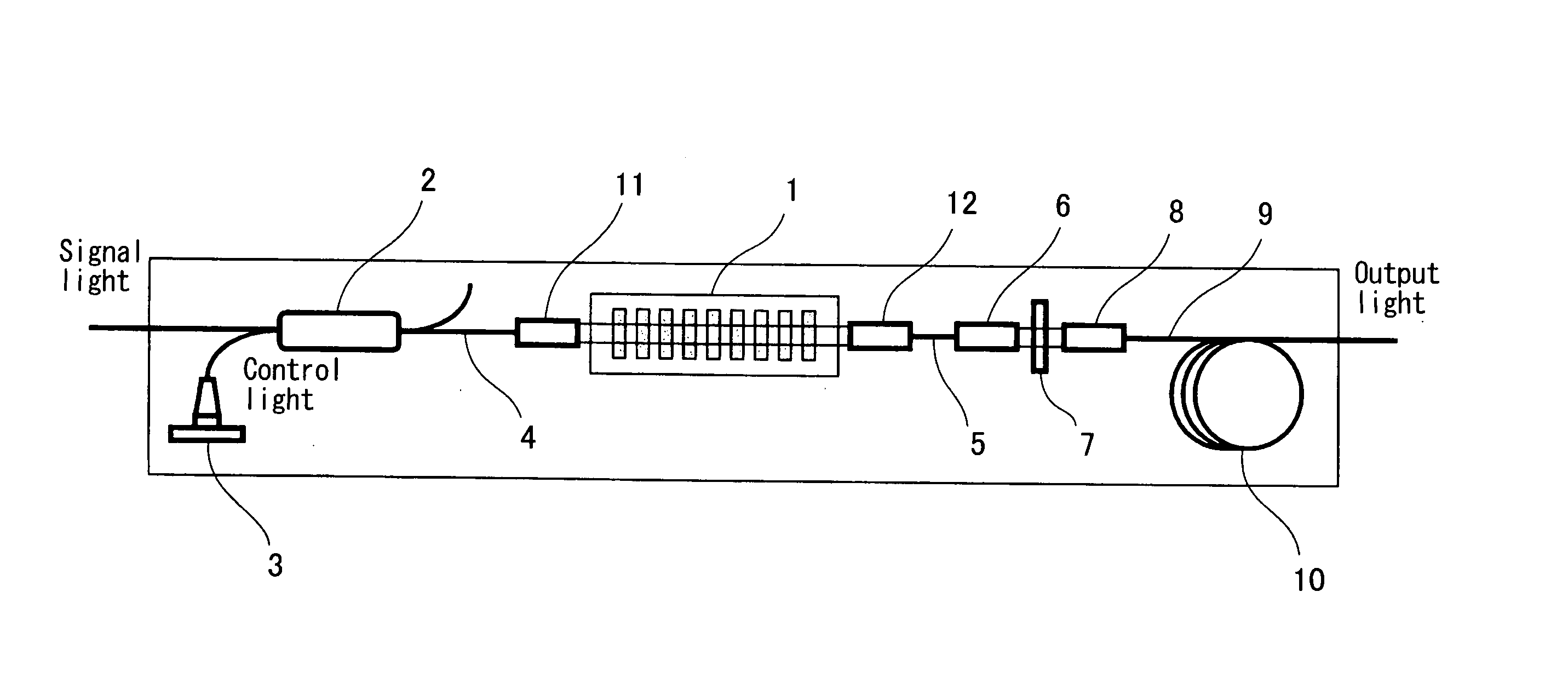
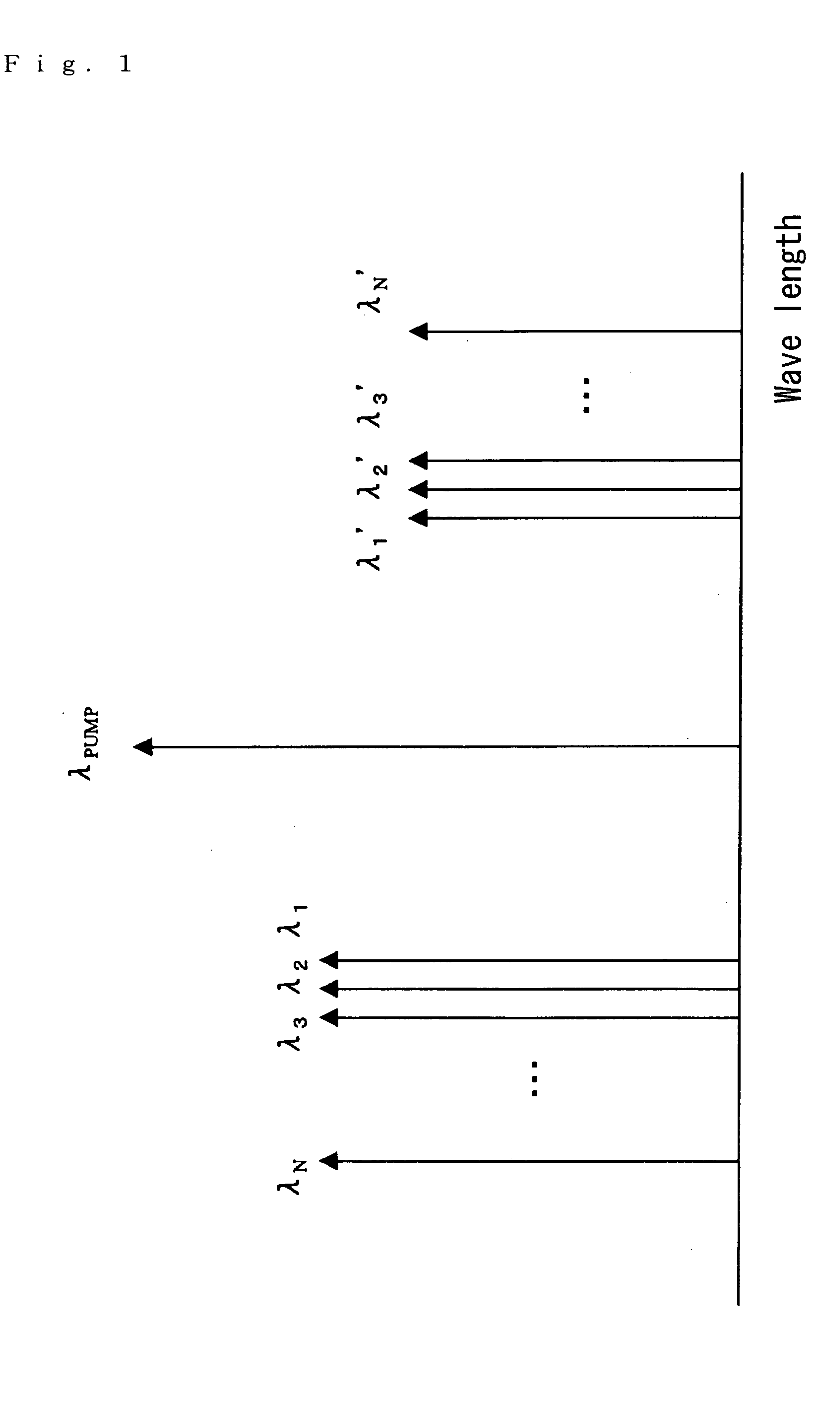
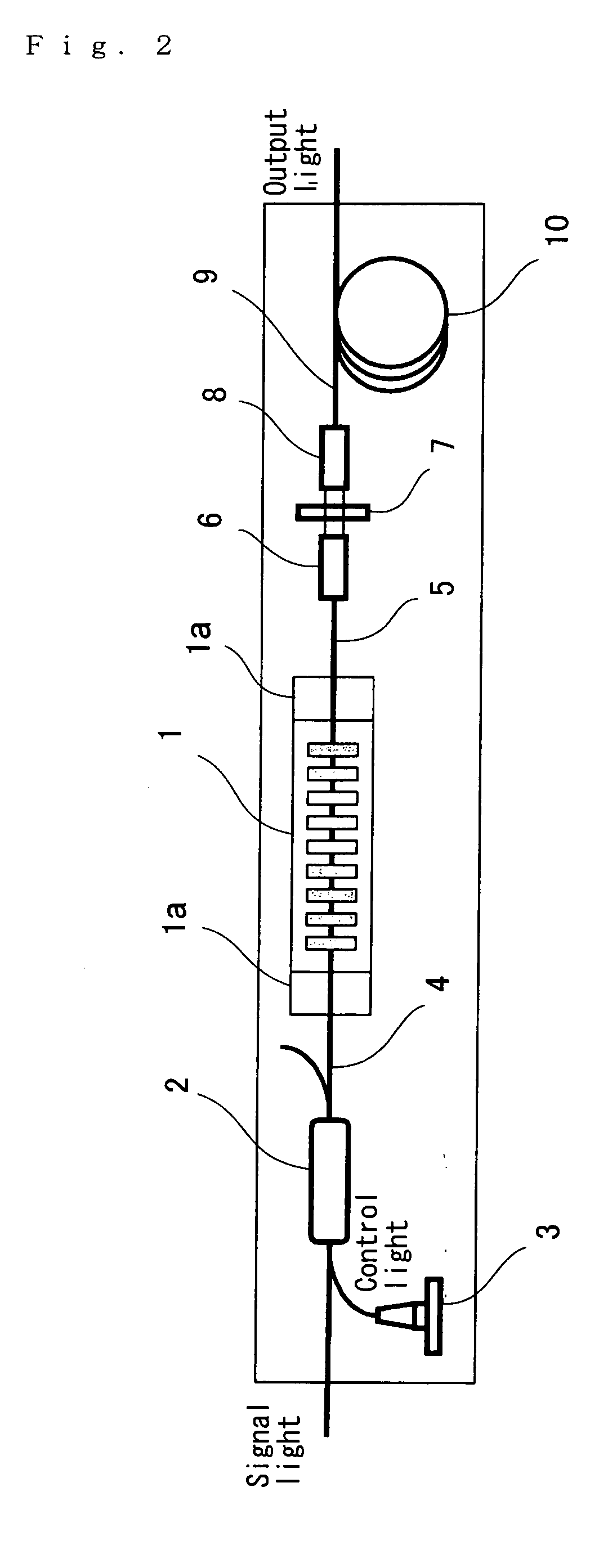
[0044]FIG. 2 is a schematic structural diagram which shows a WDM wavelength converter constituting a first working configuration of the present invention. In FIG. 2, an optical waveguide structure is formed in a quasi-phase matched quartz crystal 1, and V grooves 1a are formed before and after this structure. Below, a case in which a C-L inter-band wavelength conversion is performed will be described as an example. In this case, if the wavelength λpump of the control light is set so that λpump=0.785 μm, the signal light λin=1.53 to 1.57 m, and the output light λout=1.57 to 1.61 μm. Furthermore, the wavelength bands of the signal light and output light may also be the reverse of the bands described above.

[0045] In FIG. 2, the signal light that is guided by the single-mode optical fiber is coupled with control light that is emitted from a laser d...


PUM

PropertyMeasurementUnit
wavelengthaaaaaaaaaa

Abstract

The signal light is coupled with control light that is emitted from a laser diode 3 by a WDM coupling device 2. The optical fiber 4 on one end of the WDM coupling device is mode-matched with the optical waveguide of the quasi-phase matched quartz crystal 1 by a V groove 1a. The output light generated by the difference frequency generation of the signal light and control light is again guided to the optical fiber 5 from the quasi-phase matched quartz crystal 1 by the other V groove 1a. Then, this light is incident on the optical filter 7, so that the signal light and control light are cut. The optical fiber 9 is connected to a fiber amplifier 10. In cases where a quasi-phase matched quartz crystal is used as the wavelength conversion element, the wavelength conversion efficiency drops compared to lithium niobate as a result of the nonlinear constants being small. The fiber amplifier 10 is installed in order to compensate for this. As a result, a wavelength converter for use in optical communications can be obtained which shows little problem of optical damage, which can be used at a broad range of temperatures, and which also has good coupling characteristics with quartz type optical fibers.

Description

TECHNICAL FIELD [0001] The present invention relates to an optical wavelength converter which is used in an optical communication system that utilizes wavelength multiplexing. BACKGROUND ART [0002] In the field of optical communications, Dense Wavelength Division Multiplexing (DWDM) in which signals are multiplexed by being carried on a plurality of different wavelengths are generally used in order to handle added communications capacity. In such a field, optical wavelength conversion between the respective nodes of the network will be indispensable in the future for the effective utilization of the limited wavelength resources of the respective nodes. In the past, furthermore, wavelength multiplex communications have been performed only in the C band; however, there are prospects for the use of other wavelength bands as a result of the increase in communication capacity. Accordingly, a need has arisen for inter-band wavelength conversion between the respective nodes of such network...

Claims


Application Information

Patent Timeline
Patent Type & Authority Applications(United States)
IPC IPC(8): G02F1/35G02F1/377
CPCG02F1/3534G02F1/3558G02F1/3544
Inventor KURIMURA, SUNAOHARADA, MASAKI
Owner NAT INST FOR MATERIALS SCI
Why Eureka
Try Eureka