
Method for manufacturing a transmitting optical sub-assembly with a thermo-electric cooler therein

a technology of thermo-electric cooler and transmitting optical sub-assembly, which is applied in the direction of semiconductor lasers, semiconductor/solid-state device testing/measurement, instruments, etc., can solve the problems of limiting the limiting the cooling capacity of the thermo-electric cooler, and increasing the power consumption of the semiconductor device to operate in stable high-speed signal operation

Active Publication Date: 2005-09-29
SUMITOMO ELECTRIC IND LTD
View PDF11 Cites 40 Cited by
  • Summary
  • Abstract
  • Description
  • Claims
  • Application Information

AI Technical Summary

Benefits of technology

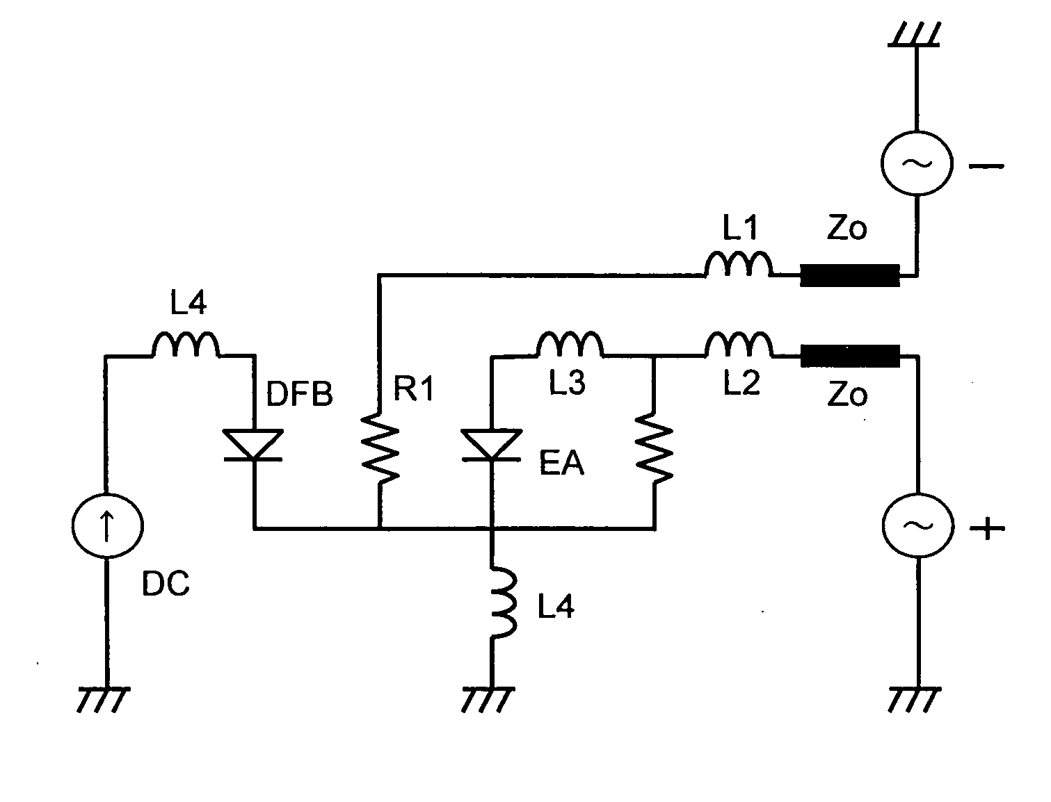
[0016] The first terminator may be connected in serial to the first transmission line or may be connected between the first transmission line and the surface ground layer. The transmitting optical sub-assembly of the invention may further comprise a second transmission line and a second terminator connected to the second transmission line. The second transmission line transmits another modulation signal with a phase opposite to the phase of the modulation signal. A first distance from light-emitting device to the first terminator may be shorter than a second distance from the light-emitting device to the second terminator. By this arrangement, the light-emitting device may be escaped from heat generated by the second terminator. On the other hand, the first terminator may be positioned immediate to the light-emitting device not to degrade the quality of the high frequency signal.
[0017] The transmitting optical sub-assembly may further provide a multi-layered ceramic substrate to transmit the modulation signal to the first transmission line and the another modulation signal to the second transmission line each formed on the carrier. Further, a difference between the first and second distances may be compensated on the multi-layered ceramic substrate.
[0018] Moreover, the transmitting optical sub-assembly may provide a package with a package ground. The surface ground and the inner ground connected to the surface ground is preferably isolated from this package ground. In this arrangement, the high frequency signal transmitted on the carrier can be escaped from degrading in the waveform thereof and from the noise superposed on the package ground.
[0019] The insulating carrier may be made of aluminum nitride (AlN). Since the AlN shows a good thermal conductivity, and a small heat capacity, the thermal load affected to the thermoelectric cooler can be reduced. This results in a compact sized thermoelectric cooler. Moreover, on the carrier made of AlN may be formed with the second mounting surface. A collimating lens made of glass may be directly mounted on the second mounting surface without any metallic lens holder. This configuration does not affect a large heat capacity attributed to the metallic lens holder to the thermoelectric cooler. Further, a level of the first mounting surface may be higher than a level of the second mounting surface.
[0021] The light-emitting device may be a semiconductor laser diode. In this case, the first terminator is preferably connected in serial to the first transmission line. Since the parasitic resistance of the laser diode is a range from a few ohms to over ten ohms, the first transmission line can be terminated to 50 ohm by connecting the first terminator with over ten ohms in serial to the first transmission line. According to this configuration, the high frequency modulation signal transmitting on the first transmission line can be escaped from degrading in the waveform thereof.
[0022] In a modification, the light-emitting device may be a semiconductor laser diode with a first electrode and a second electrode. The first and second transmission lines may be formed on the carrier, and the first and second terminator may be formed on the carrier. The first terminator is connected to the first electrode of the laser diode, while the second terminator is connected to the second electrode of the laser diode. The modulation signal may be provided in the first transmission line, while on the second transmission line may be provided with another modulation signal whose phase is opposite to that of the modulation signal. Thus configured differential mode driving can operate the laser diode in further stable at the high frequencies.

Problems solved by technology

On the other hand, as the transmission speed increases, the power consumption of semiconductor devices also increases to operate in stable for the high-speed signal.
The direct modulation for the LD can not satisfy such high quality specification,
To obtain small-sized optical assembly, it will be necessary to have the thermoelectric cooler small, but it will restrict the capacity of the cooling of the thermoelectric cooler.
However, the CuW has relatively large heat capacity.
Furthermore, in the EA-DFB device, in particular, the EA portion and the DFB portion are integrated to each other, the high frequency signal applied to the EA portion has leaked to the DFB device that is inherently driven by the DC signal.
However, the EA-DFB device is installed within the package, the ground line can not widen and shorten enough due to less space within the package, which makes the ground line the common impedance to the EA portion and the DFB portion.
Therefore, the high frequency signal applied to the EA portion appears in deformed, so the optical output because the EA portion is driven by this deformed signal, which increases the jitter and the noise involved in the optical output.
Moreover, in products intended to operate in the high speed, how the dynamic testing can be performed dominates not only the performance of the products but also the cost thereof.
However, once deciding the failure for the product, all parts must be scraped although the failure is attributed to only a portion of parts.
On the other hand, when the dynamic testing is carried out during the production, the reliability of the testing itself may not be secured due to the difference between the final and the intermediate configurations.

Method used


Image

  • Method for manufacturing a transmitting optical sub-assembly with a thermo-electric cooler therein
  • Method for manufacturing a transmitting optical sub-assembly with a thermo-electric cooler therein
  • Method for manufacturing a transmitting optical sub-assembly with a thermo-electric cooler therein

Examples


Embodiment Construction

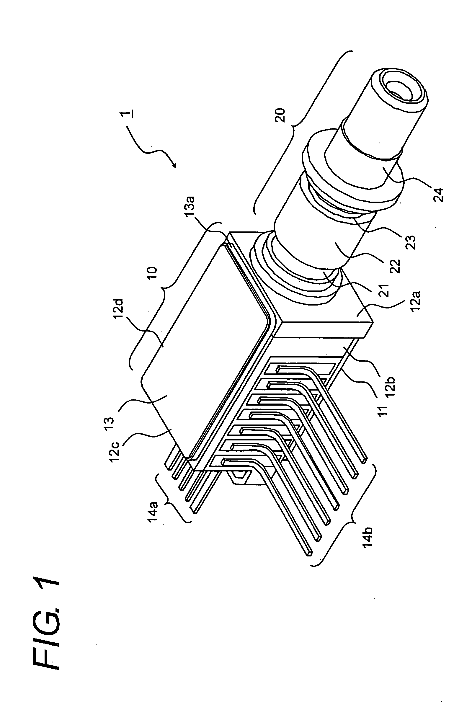
[0037]FIG. 1 illustrates an external appearance of the optical transmitting assembly of the present invention.

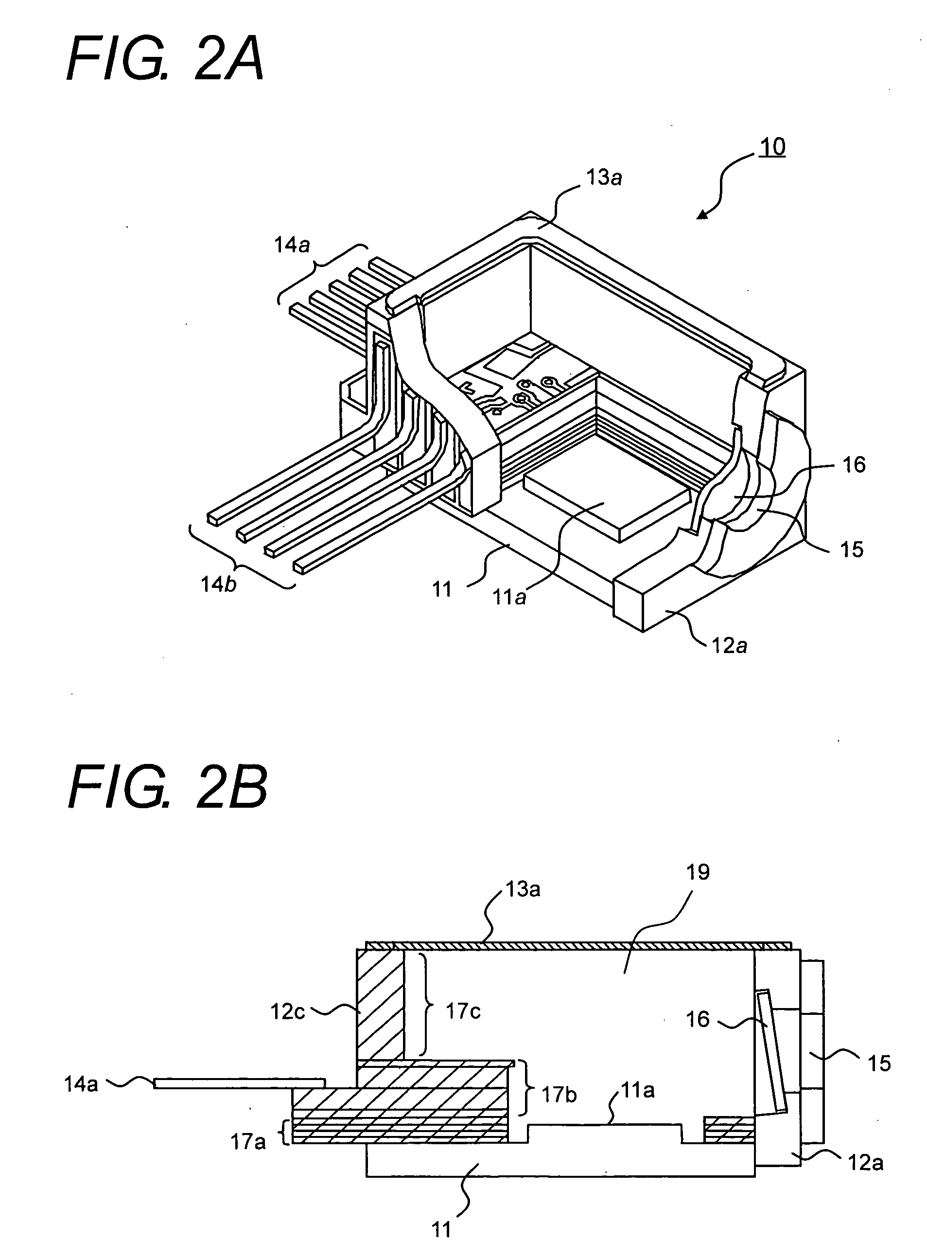
[0038] The optical transmitting assembly includes a box-shaped package 10 and an optical coupling portion 20 attached to one side wall 12a of the package 10. The package 10 has, so called, a butterfly shape with a bottom 11, four side walls 12a to 12d disposed on the bottom 11, and a ceiling 13. One side wall 12a provides the optical coupling portion 20. The other side wall 12c opposite to this side wall 12a arranges lead pins 14a. These lead pins 14a are to provide a high-frequency modulation signal to a semiconductor optical device installed within the optical transmitting assembly. Further, in the third wall 12b intersecting the first wall 12a and the second wall 12c facing the first wall 12a also arranges a plurality of lead pins 14b, through which DC signals or low frequency signals, such as the electric power to an thermoelectric cooler, an output from a temperature s...


PUM


Abstract

The present invention relates to an optical transceiver that installs an optical transmitting assembly and an optical receiving assembly both are compact, inexpensive, and capable of operating at a high speed. The optical transmitting assembly of the present invention provides the metal bottom that installs the thermoelectric cooler thereon and the semiconductor optical device is mounted, via the insulating substrate, on the thermoelectric cooler. The first and second multi-layered ceramic substrates are provided to surround the thermoelectric cooler. The DC signal or the low-frequency signal for the thermoelectric cooler and the semiconductor optical device is supplied through the first ceramic substrate, while the high frequency signal for the semiconductor device, with the complementary signal having the opposite phase to the high frequency signal, is provided to the semiconductor device through the inner layer of the second ceramic substrate and the insulating substrate. The semiconductor light-receiving device, which monitors light emitted from the semiconductor light-emitting device, is mounted on the top layer of the second ceramic substrate. Thus, the transmission path for the high frequency signal from the drive circuit installed outside of the transmitting assembly to the light-emitting device becomes substantially linear.

Description

CROSS REFERENCE TO RELATED APPLICATIONS [0001] The present application claims benefit of prior filed provisional applications Ser. No. 60 / 545,504, filed Feb. 19, 2004, Ser. No. 60 / 592,527, filed Aug. 2, 2004, and Ser. No. 60 / 632,716, filed Dec. 3, 2004.BACKGROUND OF THE INVENTION [0002] 1. Field of the Invention [0003] The present invention relates to an optical transmitting assembly used in high-speed optical communication (for example, 10 Gbps) that provides a temperature control function within a small sized package. [0004] 2. Related Prior Art [0005] The optical communication strongly requests an optical transceiver applicable to the high-speed transmission with a miniaturized package. For example, a multi-source agreement (MSA) has been standardized for the miniaturized optical transceiver with a pluggable function at the transmitting speed of 10 Gbps. This standard rules to provide an optical receptacle capable of mating with a dual LC-typeM optical connector. The pitch betwee...

Claims


Application Information

Patent Timeline
Patent Type & Authority Applications(United States)
IPC IPC(8): G01R31/26G01R31/28G02B6/34G02B6/42H01L21/50H01L21/66H01S5/02H01S5/022H01S5/024
CPCG02B6/4201G02B6/4204G02B6/4246G02B6/4292H01S5/02415H01S5/02248H01S5/02276H01S5/02284H01S5/02216G02B6/4272G02B6/4271G02B6/4279H01S5/02325H01S5/02345H01S5/02251
Inventor KIHARA, TOSHIAKIGO, HISAOKATO, KIYOSHI
Owner SUMITOMO ELECTRIC IND LTD
Learn More