Method for producing semiconductor light emitting device, method for producing semiconductor device, method for producing device, method for growing nitride type III-V group compound semiconductor layer, method for growing semiconductor layer, and method for growing layer

a technology of nitride type iiiv group and semiconductor, which is applied in the direction of crystal growth process, polycrystalline material growth, semiconductor laser, etc., can solve the problems of difficult to produce a large diameter sic substrate, small difference of lattice constants of sic substrates, and inability to know the proper substrate materials of devices using nitride type iii-v group compound semiconductors with high reliability. , to achieve the effect of good light characteristi

Inactive Publication Date: 2005-10-06
SUMITOMO ELECTRIC IND LTD +1
View PDF9 Cites 14 Cited by
  • Summary
  • Abstract
  • Description
  • Claims
  • Application Information

AI Technical Summary

Benefits of technology

[0026] Therefore, in view of the foregoing, it would be desirable to provide a semiconductor light emitting device that has good characteristics such as g

Problems solved by technology

However, proper substrate materials for devices using nitride type III-V group compound semiconductors that have high reliability are not known.
A SiC substrate having a small difference of lattice constants is expensive.
In addition, it is difficult to produce a SiC substrate having a large diameter.
Since a tensile distortion takes place in a crystal film, it easily cracks.
In addition, there is no substrate that can lattice-match GaN.
However, lattice-mismatch of a sapphire substrate to GaN is large (around 13%).
Thus, when the nitride type III-V group compound semiconductor is used for a semiconductor laser, it does not have reliability for a long time.
In addition, (1) since a sapphire substrate does not have cleavage, an end plane of a laser cannot be stably formed with specular property.
As a result, the device forming process is adversely affected.
When a device is formed on a sapphire substrate by the ELO, in addition to the foregoing problem of bad cleavage due to characteristics of sapphire, there are for example the following problems.
(2) Since the crystal film thickness increases for the ELO, the subs

Method used


Image

  • Method for producing semiconductor light emitting device, method for producing semiconductor device, method for producing device, method for growing nitride type III-V group compound semiconductor layer, method for growing semiconductor layer, and method for growing layer
  • Method for producing semiconductor light emitting device, method for producing semiconductor device, method for producing device, method for growing nitride type III-V group compound semiconductor layer, method for growing semiconductor layer, and method for growing layer
  • Method for producing semiconductor light emitting device, method for producing semiconductor device, method for producing device, method for growing nitride type III-V group compound semiconductor layer, method for growing semiconductor layer, and method for growing layer

Examples


tenth embodiment

(Tenth Embodiment)

[0320] Next, a tenth embodiment of the present invention will be described.

[0321] As shown in FIG. 24, according to the tenth embodiment, upper portions of regions B of a GaN substrate 1 are etched out as with the first embodiment. In this case, the etched-out depth is as large as for example several ten μm. Thereafter, as shown in FIG. 25, an insulation film 18 such as a SiO2 film is fully formed on the surface of the GaN substrate 1. At that point, since the etched-out portions of the regions B are deep, they are not fully filled with the insulation film 18. As a result, the GaN substrate 1 has holes. Thereafter, the insulation film 18 is etched back by for example the RIE method so as to remove the insulation film 18 from the region A. Thereafter, a GaN type semiconductor layer L is grown on the GaN substrate 1 as with the fifth or sixth embodiment.

[0322] Except for the foregoing portion, the tenth embodiment is the same as the first embodiment. Thus, the desc...

eleventh embodiment

(Eleventh Embodiment)

[0324] Next, an eleventh embodiment of the present invention will be described.

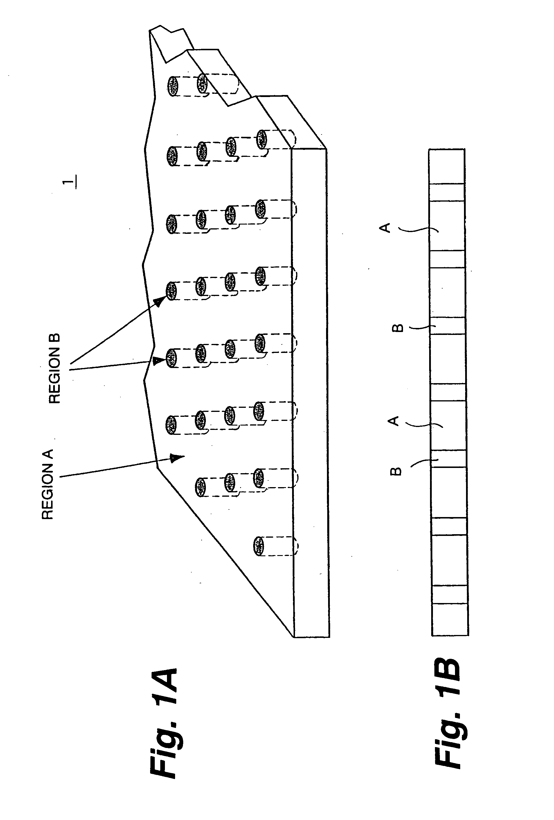
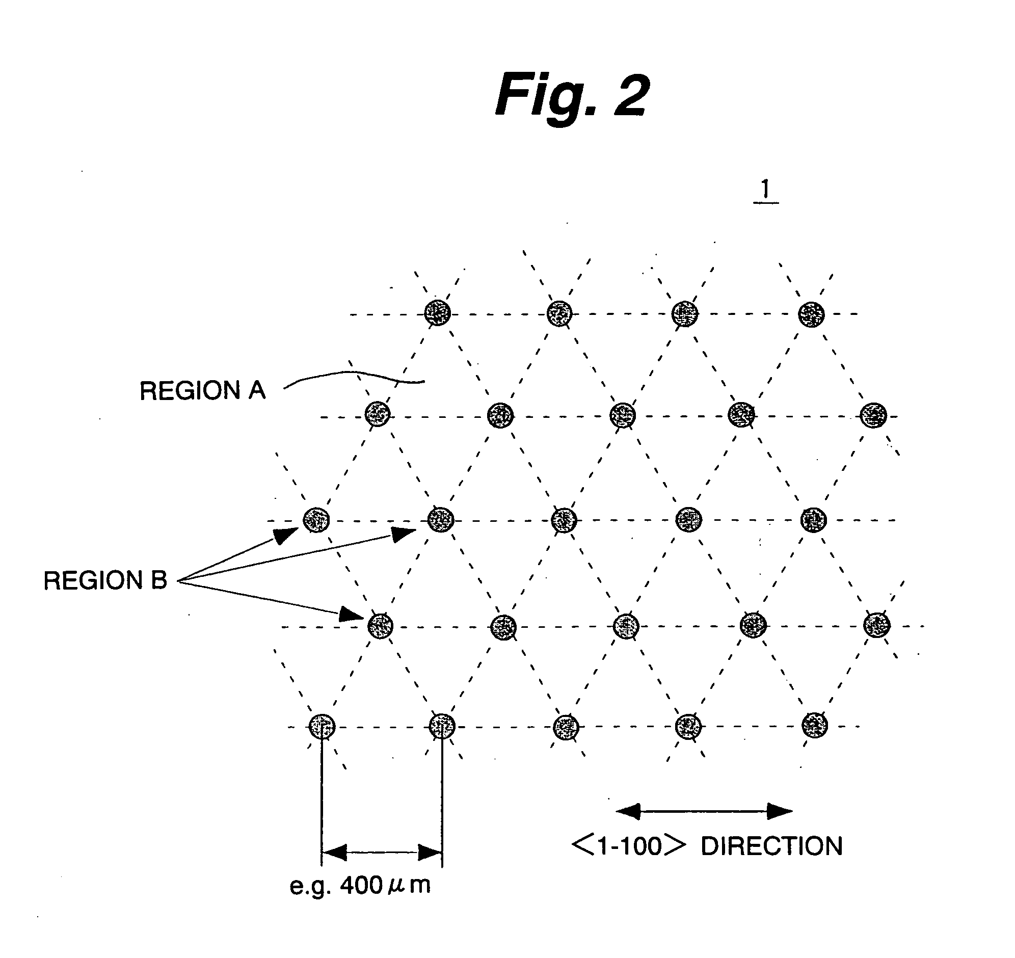
[0325] As shown in FIG. 27, according to the eleventh embodiment, regions B are periodically arranged in a hexagonal lattice shape in an area A of a GaN substrate 1 as with the first embodiment. However, regions C are formed as transitional regions between the region A and the regions B unlike with the first embodiment. The average dislocation density of the regions C is in the middle of the average dislocation density of the region A and the average dislocation density of the regions B. In reality, the average dislocation density of the region A is 2×106 cm−2 or lower. The average dislocation density of the regions B is 1×108 cm−2 or greater. The average dislocation density of the regions C is smaller than 1×108 cm−2 and greater than 2×106 cm−2, for example around (1 to 2)×107 cm−2. The arrangement period of the regions B (the distance between the centers of the most adjacent region...

twelfth embodiment

(Twelfth Embodiment)

[0329] Next, a twelfth embodiment of the present invention will be described.

[0330] Unlike with the second embodiment of which all the regions B of the GaN substrate 1 are etched out, according to the twelfth embodiment, all regions B and regions C of a GaN substrate 1 are etched out.

[0331] Except for the foregoing portion, the twelfth embodiment is the same as the first embodiment. Thus, the description of the other portions of the twelfth embodiment is omitted.

[0332] According to the twelfth embodiment, the same advantage as the first embodiment can be obtained.


PUM


Abstract

A method for producing a semiconductor light emitting device is disclosed. The method comprises the step of growing a nitride type III-V group compound semiconductor layer that forms a light emitting device structure on a principal plane of a nitride type III-V group compound semiconductor substrate on which a plurality of second regions made of a crystal having a second average dislocation density are regularly arranged in a first region made of a crystal having a first average dislocation density so as to produce a semiconductor light emitting device, the second average dislocation density being greater than the first average dislocation density. The nitride type III-V group compound semiconductor layer does not directly contact the second regions on the principal plane of the nitride type III-V group compound semiconductor substrate.

Description

BACKGROUND OF THE INVENTION [0001] 1. Field of the Invention [0002] The present invention relates to a method for producing a semiconductor light emitting device, a method for producing a semiconductor device, a method for producing a device, a method for growing a nitride type III-V group compound semiconductor layer, a method for growing a semiconductor layer, and a method for growing a layer. In particular, the present invention relates to for example those suitable for producing a semiconductor laser, a light emitting diode, or an electron traveling device using a nitride type III-V group compound semiconductor. [0003] 2. Description of the Related Art [0004] Nitride type III-V group compound semiconductors such as GaN, AlGaN, GaInN, and AlGaInN feature in a large band gap Eg and direct transition semiconductor materials in comparison with arsenic type III-V group compound semiconductors such as AlGaInAs and phosphorous type III-V group compound semiconductors such as AlGaInP. T...

Claims


Application Information

Patent Timeline
IPC IPC(8): C30B25/02C30B29/40H01L21/00H01L21/20H01L29/221H01L33/00H01S5/02H01S5/20H01S5/22H01S5/223H01S5/30H01S5/32H01S5/343
CPCB82Y20/00C30B25/02C30B29/403H01L21/02389H01L21/0243H01L21/0254H01L21/02658H01L33/007H01S5/0202H01S5/2004H01S5/2214H01S5/2231H01S5/3063H01S5/3215H01S5/34333H01S2301/173H01S2304/04H01S2304/12
Inventor YANASHIMA, KATSUNORIMOTOKI, KENSAKU
Owner SUMITOMO ELECTRIC IND LTD
Why Eureka
Try Eureka