
Plasma resistant member

a technology ceramic sintered body, which is applied in the field of plasma resistant member, can solve the problems of compromising the performance and reliability of a semiconductor, adversely affecting the accuracy of etching, and the gradual corrosion of the plasma resistant member as described above, so as to prevent cracks from generating

Inactive Publication Date: 2005-10-13
COVALENT MATERIALS CORP
View PDF4 Cites 77 Cited by
  • Summary
  • Abstract
  • Description
  • Claims
  • Application Information

AI Technical Summary

Benefits of technology

[0012] Accordingly, it is an object of the present invention carried out for solving the foregoing problems to provide a plasma resistant material that is mechanically reinforced and is sufficiently durable to exposure to a low pressure high density plasma.
[0028] Sintered bodies of the oxide or composite oxide of the Group. IIIA element is highly resistant to corrosion due to the following reasons. A fluoride of the group IIIA element is formed when the oxide or composite oxide of the group IIIA element is exposed to a fluorine gas. Since the fluoride of the Group IIIA element is hardly evaporated off due to its high melting point or its high boiling point, besides the fluoride layer prevents a reaction with a fluoride radical from advancing, thereby exhibiting a high corrosion resistance.
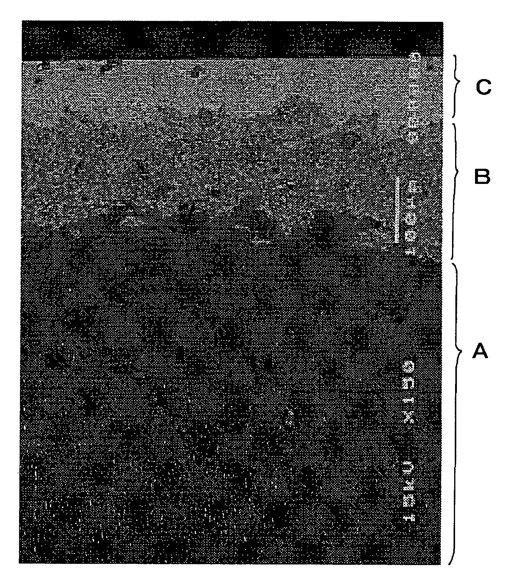
[0030] The first, second and third aspects of the present invention were obtained, through intensive studies, by taking notice of the facts that cracks can be prevented from generating by relaxing the difference in the thermal expansion ratio by allowing an intermediate layer that serves as an absorbing layer to exist between the surface of the alumina based material and the sintered body of the oxide or composite oxide of the group IIIA element.
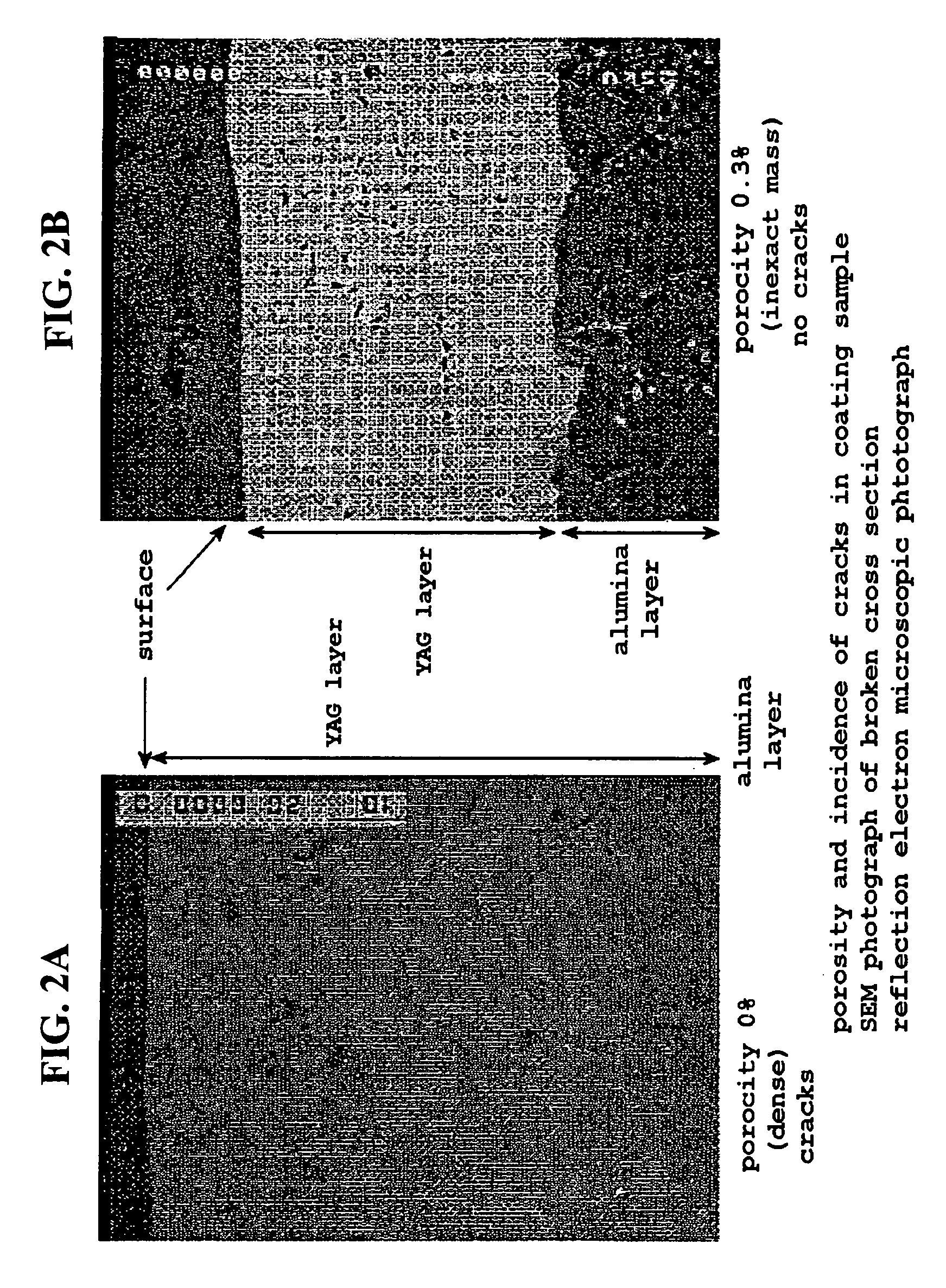
[0031] Furthermore, the fourth aspect of the present invention was achieved by finding that cracks can be prevented from generating without providing an intermediate layer between the alumina based material and the sintered body of the oxide or composite oxide of the group IIIA element, when the porosity in the sintered body of the oxide or composite oxide of the group IIIA element on the surface falls within a specified range.

Problems solved by technology

However, the plasma resistant member comprising a ceramic sintered body as described above is gradually corroded by being exposing with the plasma under the corrosive gas atmosphere to affect etching conditions due to changes of surface properties such as elimination of crystalline particles constituting the surface of the member.
In other words, eliminated particles are adhered on the wafer 7 and lower electrode 8 and the like to adversely affect the accuracy of etching, thereby compromising performance and reliability of a semiconductor.
However, while the yttrium aluminum garnet sintered body is excellent in plasma resistance, it has poor mechanical strength such as bending strength and fracture toughness.
Poor mechanical strength (e.g brittleness) as used herein means that the member is liable to be damaged or fractured during handling such as attachment of the member in the etching apparatus.
Therefore, it was a problem that the manufacturing cost of the manufacturing apparatus itself or the manufacturing cost of semiconductors become high in addition to a relatively high expense for the row material.

Method used


Image

  • Plasma resistant member
  • Plasma resistant member
  • Plasma resistant member

Examples


first embodiment

[0036] The first embodiment of the present invention will de described hereinafter.

[0037] An intermediate layer comprising 10 to 80% by weight of an oxide or a composite oxide of a group IIIA element in the periodic table and 90 to 20% by weight of alumina is formed between an alumina based material and a layer of a sintered body as a surface layer containing the oxide or composite oxide of the group IIIA element in the periodic table in this embodiment.

[0038] The alumina based material in this embodiment is a sintered body of alumina (alumina based ceramic) comprising at least 90% by weight of alumina.

[0039] The layer of the sintered body as a surface layer containing the oxide or composite oxide of the group IIIA element in the periodic table for covering the surface of the alumina based material to be exposed to a plasma comprises, for example, an oxide of Sc, Y, Er, La, Ce, Ne, Yb, Dy, Eu or Lu, or a composite oxide mainly comprising these elements.

[0040] Examples of the com...

second embodiment

[0048] The second embodiment of the present invention will be described hereinafter.

[0049] According to this embodiment, at least the surface of the alumina based material exposed to a plasma is formed of a surface layer including an oxide or a composite oxide of a group IIIA element in the periodic table via an intermediate layer, wherein the content of the oxide or composite oxide of the group IIIA element in the periodic table is 70% by weight or more. Since corrosion resistance becomes insufficient when the content of the oxide or composite oxide of the group IIIA element in the periodic table in the surface layer is less than 70% by weight, the more preferable range thereof is 90% by weight or more.

[0050] It is particularly preferable that the content of the oxide or composite oxide of the group IIIA element in the periodic table in the intermediate layer and surface layer continuously changes in the direction of depth in each layer.

[0051] The rate of change of the content o...

third embodiment

[0057] The third embodiment of the present invention will be described hereinafter.

[0058] The difference of the thermal expansion between the alumina based material and the surface layer including an oxide or a composite oxide of a group IIIA element in the periodic table is relaxed in this embodiment by inserting an intermediate layer having a dense structure between the alumina based material and the surface layer including an oxide or a composite oxide of a group IIIA element in the periodic table, thereby enabling a coating member free from cracks to be manufactured.

[0059] A remnant stress is generated due to a difference of linear expansion coefficient during firing to arise cracks in the fired body when alumina is coated with a layer comprising an oxide or a composite oxide of a group IIIA element in the periodic table having a porosity of 0.1% or less. For avoiding cracks from generating, an inexact mass ceramic layer having a porosity of 0.2 to 5% is used as the intermedia...


PUM

PropertyMeasurementUnit
Temperatureaaaaaaaaaa
Lengthaaaaaaaaaa
Fractionaaaaaaaaaa

Abstract

The present invention provides a plasma resistant member having a reinforced mechanical strength and being sufficiently durable to exposure to a low pressure high density plasma. At least the surface of the alumina based material is formed of an oxide or composite oxide layer of a group IIIA element via an intermediate layer. It is preferable in the construction of the plasma resistant member that the intermediate layer comprises 10 to 80% by weight of the oxide or composite oxide of the group IIIA element in the periodic table and 90 to 20% by weight of alumina. The intermediate layer may also comprise a course ceramic with a porosity of 0.2 to 5%. It is also desirable that at least one of the conditions such as a difference in the thermal shrinkage ratio at 1600 to 1900° C. of 3% or less is provided.

Description

BACKGROUND OF THE INVENTION [0001] 1. Field of the Invention [0002] The present invention relates to a plasma resistant member. In particular, the present invention relates to a plasma resistant member having an excellent plasma resistance under a halogen based corrosive gas atmosphere. [0003] 2. Description of the Related Art [0004] An etching apparatus and a sputtering apparatus that apply fine processing on a semiconductor wafer, or a CVD apparatus that deposits a film on the semiconductor wafer are used in the process for manufacturing a semiconductor device. Such manufacturing apparatus is provided with a plasma generation mechanism in order to form highly integrated circuits. These apparatuses include, for example, a helicon wave plasma etching apparatus as illustrated in the cross section in FIG. 4. [0005] In FIG. 4, the reference numeral 1 denotes an etching processing chamber comprising an etching gas feed port 2 and evacuation port 3, and an antenna 4, an electromagnet 5 a...

Claims


Application Information

Patent Timeline
IPC IPC(8): H05H1/46B32B18/00C04B35/44C04B35/50C04B35/505C04B41/52C04B41/89C23C14/00C23C16/44H01J37/32H01L21/205H01L21/302
CPCB32B18/00C04B2237/704C04B35/50C04B35/505C04B41/009C04B41/52C04B41/89C04B2111/00405C23C16/4404H01J37/32477H01J37/32559C04B35/44C04B2237/366C04B2237/365C04B2237/343C04B2237/34C04B2235/6567C04B2235/656C04B35/63416C04B41/4539C04B41/5031C04B41/5045C04B41/5032C04B41/522C04B35/10
Inventor UCHIMARU, TOMONORIMURAYAMA, HARUOTANAKA, TAKASHIMORITA, KEIJIMIYAZAKI, AKIRA
Owner COVALENT MATERIALS CORP
Learn More