
SOI structure having a sige layer interposed between the silicon and the insulator

a technology of silicon and insulator, which is applied in the direction of semiconductor devices, electrical equipment, transistors, etc., can solve the problems of pn junction isolation between adjacent devices on bulk silicon substrates, inconvenient high-voltage applications, and integrated circuits, so as to increase the breakdown voltage and thereby the drain current

Inactive Publication Date: 2005-11-03
SUMITOMO MITSUBISHI SILICON CORP +1
View PDF5 Cites 98 Cited by
  • Summary
  • Abstract
  • Description
  • Claims
  • Application Information

AI Technical Summary

Benefits of technology

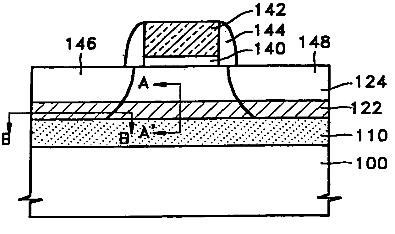
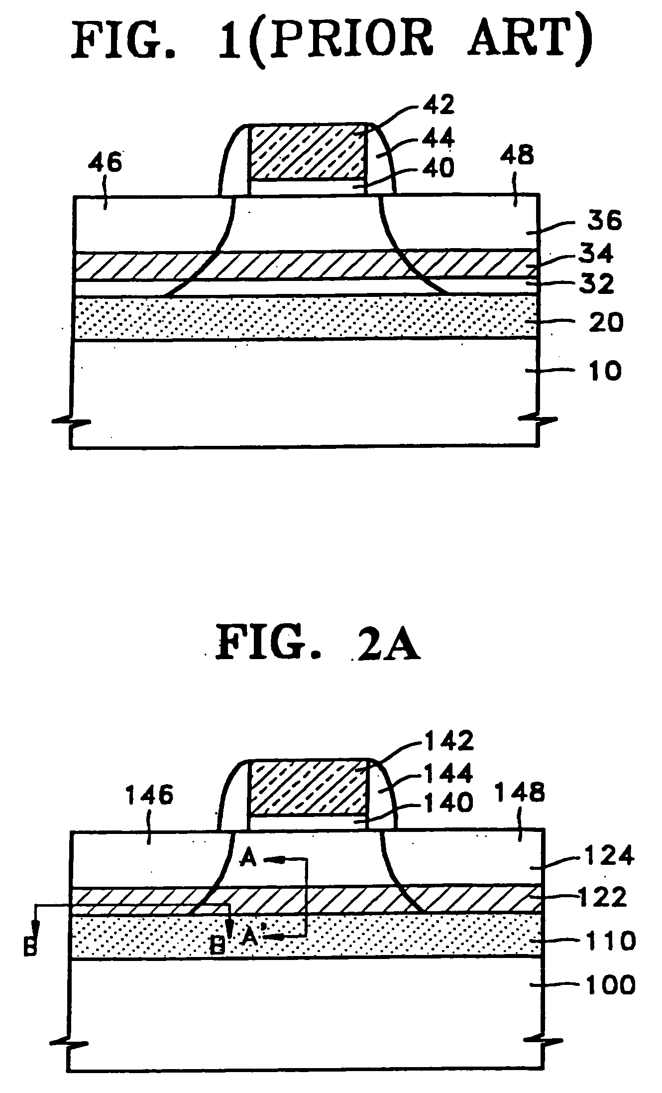
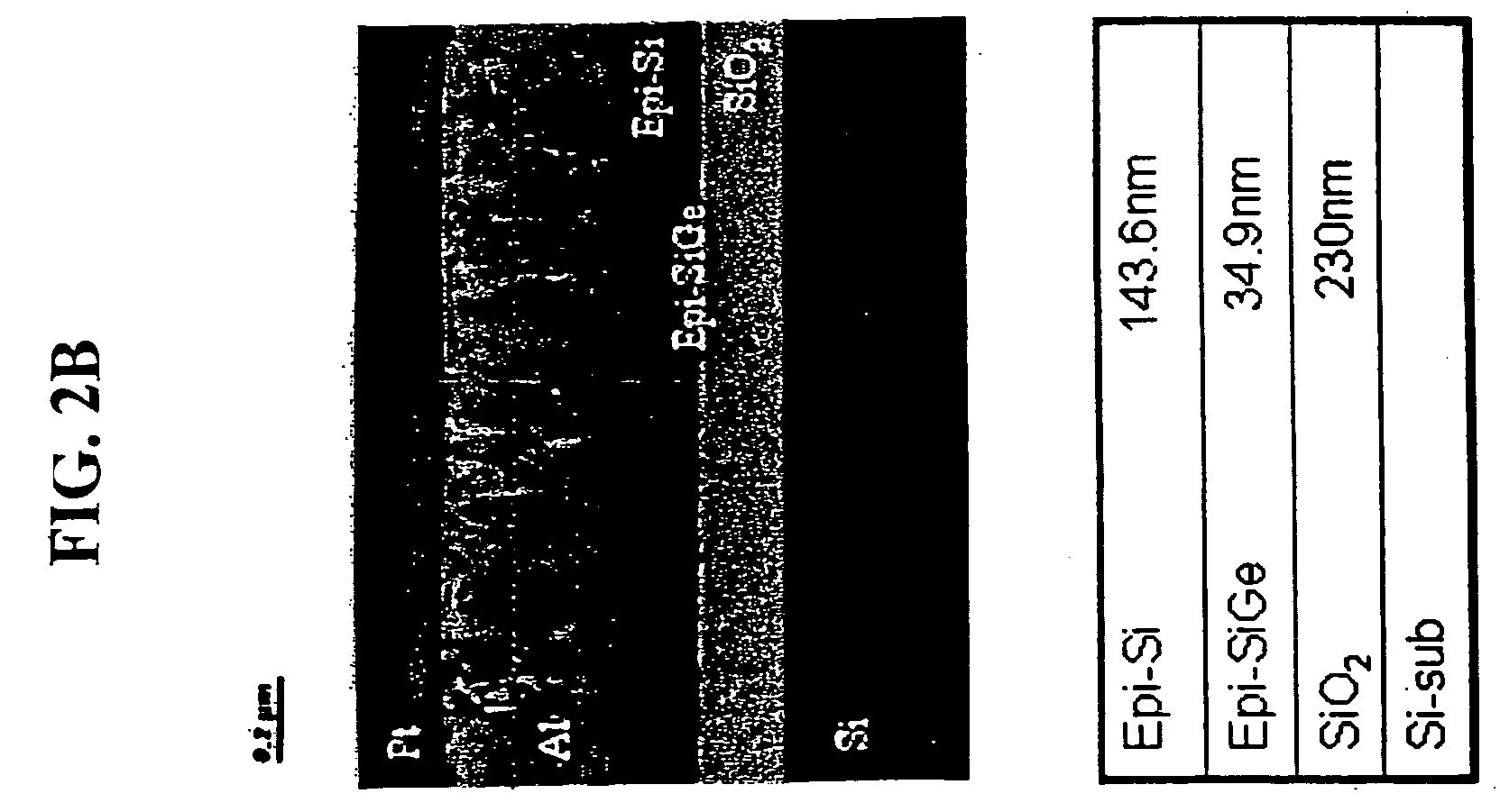
[0012] One object of the present invention is to provide a silicon on insulator (SOI) structure having a silicon germanium (SiGe) layer interposed between the silicon and the insulator. The silicon germanium layer, due to the narrow band gap characteristics of the SiGe material, suppresses both the floating body effect and the associated kink effect and increases the breakdown voltage (and thereby the drain current) of a drain in a MOS transistor formed on the SOI structure.
[0013] Another object of the present invention is to provide a SOI structure such that semiconductor devices fabricated on the SOI structure have improved transconductance and higher switching speeds as compared to devices on conventional SOI wafers.
[0017] In one embodiment of this method, the first substrate is formed of silicon, and the impurity ions implanted in the first substrate are hydrogen ions, thus facilitating separation of the first substrate from the SiGe layers. The first SiGe layer is formed to a thickness of 10-30 Å, and the projected range of the impurity ions implanted during impurity ion implantation is 50-100 Å below the first SiGe layer. After removal of the remaining first SiGe layer, the second substrate may be annealed in a hydrogen atmosphere in order to make the surface thereof smooth.

Problems solved by technology

PN junction isolation between adjacent devices on a bulk silicon substrate is used in the manufacture of silicon integrated circuits, but is not suitable for high voltage applications since junction breakdowns occur at supply voltages of about ±30 V under appropriate doping level and dimensions.
Furthermore, PN junction isolation between the adjacent devices is not effective in a radioactive environment due to transient photocurrent caused by gamma rays at the PN junction.
Despite the advantages described above, metal-oxide-semiconductor (MOS) field effect transistors (FETs) formed on a SOI wafer have a problem in that a floating body effect occurs because a buried oxide layer isolates the body of the transistor from the silicon substrate.
The increased body potential causes an undesirable kink effect in drain current vs. voltage curves of the NMOS transistor, and induces operation of a parasitic bipolar transistor, thereby leading to an instability of gate control over source-drain current.
However, since the MOS transistor of FIG. 1 has a partially depleted structure, it has relatively low transconductance and low switching speed.

Method used


Image

  • SOI structure having a sige layer interposed between the silicon and the insulator
  • SOI structure having a sige layer interposed between the silicon and the insulator
  • SOI structure having a sige layer interposed between the silicon and the insulator

Examples


first embodiment

[0050]FIGS. 7-12 are cross-sectional views showing a process for fabricating the SOI structure of the present invention. Referring to FIG. 7, a first SiGe layer 126 is epitaxially grown over a first substrate 140. The first substrate 140 is a monocrystalline silicon substrate used as a seed of the epitaxial growth. After loading the silicon substrate 140, having a purified surface, into a chemical vapor deposition (CVD) apparatus heated to a predetermined temperature, such as for example, 700° C., a reactive gas including silicon (e.g. Si2H6, SiH4, SiCl4 etc) is supplied with a reactive gas including germanium (e.g. GeH4, Ge2H6, etc.) to grow the first SiGe layer 126 over the silicon substrate 140. When the first SiGe layer 126 is grown to a predetermined thickness, for example, 10-50 Å, preferably, 20 Å, the Ge reactive gas ceases to be supplied, and continuously, a silicon layer, which will be a device layer 124, is epitaxially grown in situ to a thickness of several hundreds to t...

second embodiment

[0059]FIGS. 13-18 are cross-sectional views showing a process for fabricating the SOI structure of the present invention. Unlike the first embodiment, the second embodiment isolates the buried SiGe layer by separation implanted oxygen (SIMOX). The SIMOX process implants oxygen ions into a silicon substrate upon which thermal oxidation forms an intermediate insulating layer. The SIMOX techniques are described in Sadao Nakashima “High-quality Low-dose SIMOX Wafers”, IEICE TRANS ELECTRON, VOL. E80C, NO. 3, pp 364-369, March 1997, the entire contents of which are incorporated herein by reference. Further, SIMOX techniques are described in U.S. Pat. No. 6,486,037, the entire contents of which are incorporated herein by reference.

[0060] Referring to FIG. 13, a SiGe layer 126 is epitaxially grown over a substrate 140. The substrate 140 is a monocrystalline silicon substrate used as a seed of this epitaxial growth. After loading the silicon substrate 140 having a purified surface into a ch...

third embodiment

[0066]FIGS. 19-24 are cross-sectional views showing a process for fabricating the SOI structure of the present invention. Like the first embodiment, the third embodiment involves implanting hydrogen ions to form a cleavage region. The difference is that a single SiGe layer is formed.

[0067] Referring to FIG. 19, a silicon layer 124 is epitaxially grown over a first substrate 140 formed of silicon. The first substrate 140 is a monocrystalline silicon substrate used as a seed of this epitaxial growth. The silicon layer 124 is epitaxially grown to a thickness of several hundreds to thousands of angstroms, for example, 500 and 1800 Å in this embodiment. Then, the reactive gas including germanium is supplied again to epitaxially grow a SiGe layer 126 to a thickness of several hundreds to thousands of angstroms, for example, about 300 Å.

[0068] Referring to FIG. 20, a silicon oxide layer is formed on the epitaxially grown SiGe layer 126 as an insulating layer 132 to a thickness of several...


PUM


Abstract

A semiconductor structure and a method of manufacturing a silicon on insulator (SOI) structure having a silicon germanium (SiGe) layer interposed between the silicon and the insulator. According to one manufacturing method, a first SiGe layer, a silicon layer, and a second SiGe layer are epitaxially grown in sequence over a first substrate, and then an insulating layer is formed on the second SiGe layer. Then, impurity ions are implanted into a predetermined location of the first substrate underlying the first SiGe layer to form an impurity implantation region. A second substrate is bonded to the insulating layer on the first substrate. After the first substrate is separated along the impurity implantation region and removed, the first SiGe layer remaining on the surface of the separated region is removed so that the surface of the silicon layer may be exposed.

Description

CROSS-REFERENCE TO RELATED APPLICATIONS [0001] This application claims benefit of priority under 35 U.S.C. §119 to U.S. provisional application 60 / 352,260 filed on Jan. 30, 2002, the entire contents of which are incorporated by reference.BACKGROUND OF THE INVENTION [0002] 1. Field of the Invention [0003] The present invention relates to silicon-on-insulator (SOI) wafer device isolation technology, and more particularly to a method of fabricating a modified SOI structure having a buried semiconductor layer. [0004] 2. Description of the Related Art [0005] PN junction isolation between adjacent devices on a bulk silicon substrate is used in the manufacture of silicon integrated circuits, but is not suitable for high voltage applications since junction breakdowns occur at supply voltages of about ±30 V under appropriate doping level and dimensions. Furthermore, PN junction isolation between the adjacent devices is not effective in a radioactive environment due to transient photocurrent ...

Claims


Application Information

Patent Timeline
IPC IPC(8): H01L21/336H01L21/762H01L29/786
CPCH01L21/76243H01L21/76254H01L29/78687H01L29/66772H01L21/76259
Inventor PARK, JEAGUNTOMIZAWA, KENJILEE, GONSUBKAMIYAMA, EIJI
Owner SUMITOMO MITSUBISHI SILICON CORP
Learn More