

Organic light-emitting devices
a light-emitting device and organic technology, applied in the direction of discharge tube luminescnet screen, other domestic articles, natural mineral layered products, etc., can solve the problems of low external efficiency of devices, optimization of stability and efficiency of oleds, etc., to achieve low turn-on voltage, high luminance, and high efficiency
- Summary
- Abstract
- Description
- Claims
- Application Information
AI Technical Summary
Benefits of technology
Problems solved by technology
Method used
Image

Examples
example 1
[0116] Example 1 shows the synthesis of dopant complex 1. The tetradentate NNNN-type ligand was prepared according to modification of literature procedures (see Bacchi et al., InorganicaChimica Acta. 342:229, (2003); Male et al., J. Chem. Soc., Dalton Trans. 2487, (1997)).
Synthesis of Dopant Complex 1
[0117] Sodium acetate (0.077 g, 0.94 mmol) was suspended in a DMF (10 mL) solution of bidentate ligand, N,N-Bis-( 1H-pyrrol-2-ylmethylene)-ethane-1,2-diamine (0.1 g, 0.47 mmol). K2PtCl4 (0.19 g, 0.47 mmol) dissolved in DMSO (1 mL) was dropwise added to the suspension at 80° C. dropwise. The resulting yellow solution turned orange-red after being stirred at 80° C. for 4 hours. After cooling, distilled water (50 mL) was then added to the orange-red mixture to afford an orange-brown precipitate. The solid product was filtered and washed with H2O (2×10 mL) to give an orange-brown solid, which was then purified by silica gel column chromatography with CH2Cl2 as the eluent. Removal of solve...
example 2
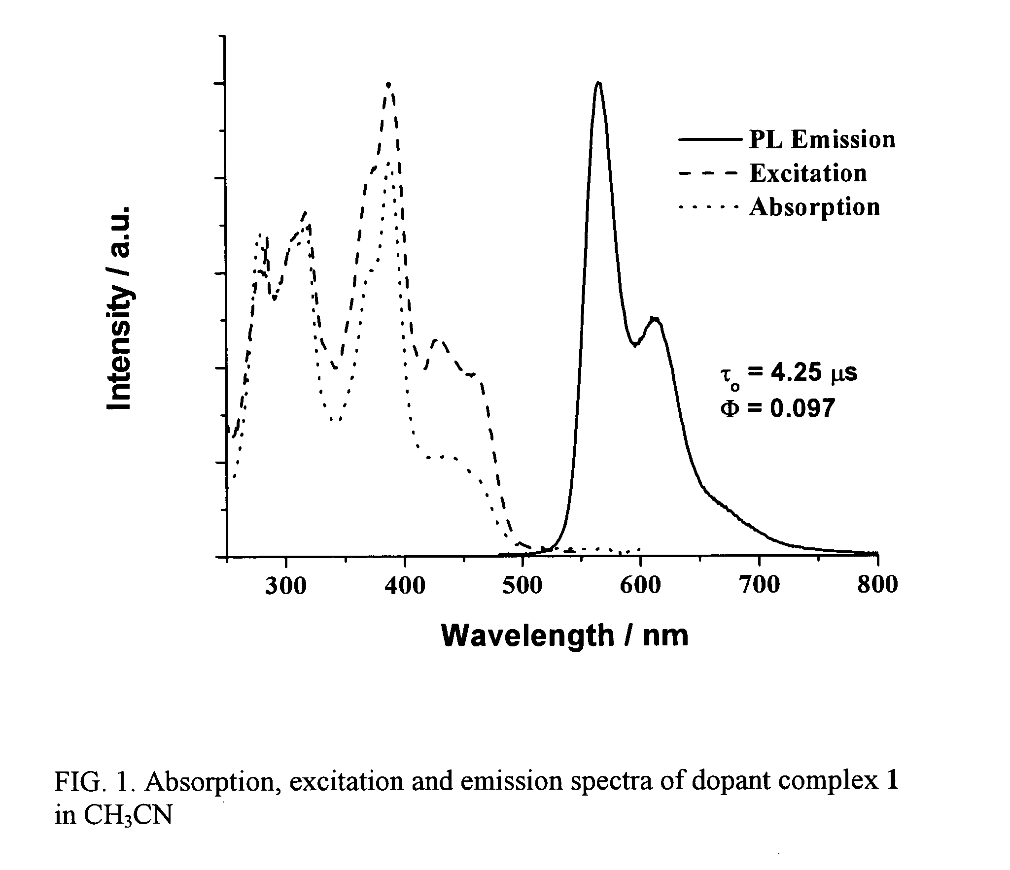
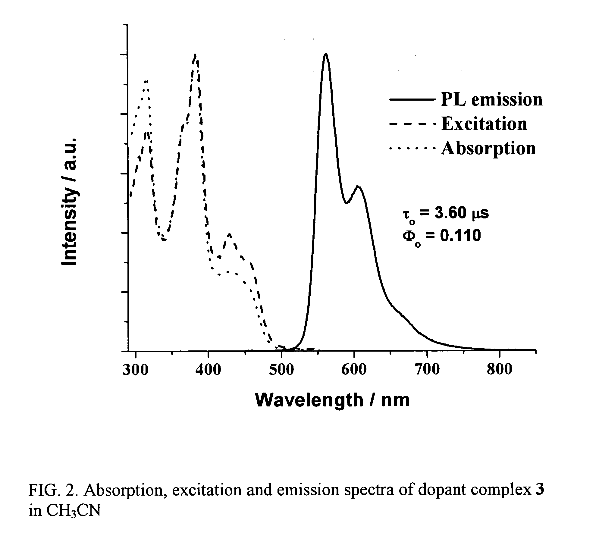
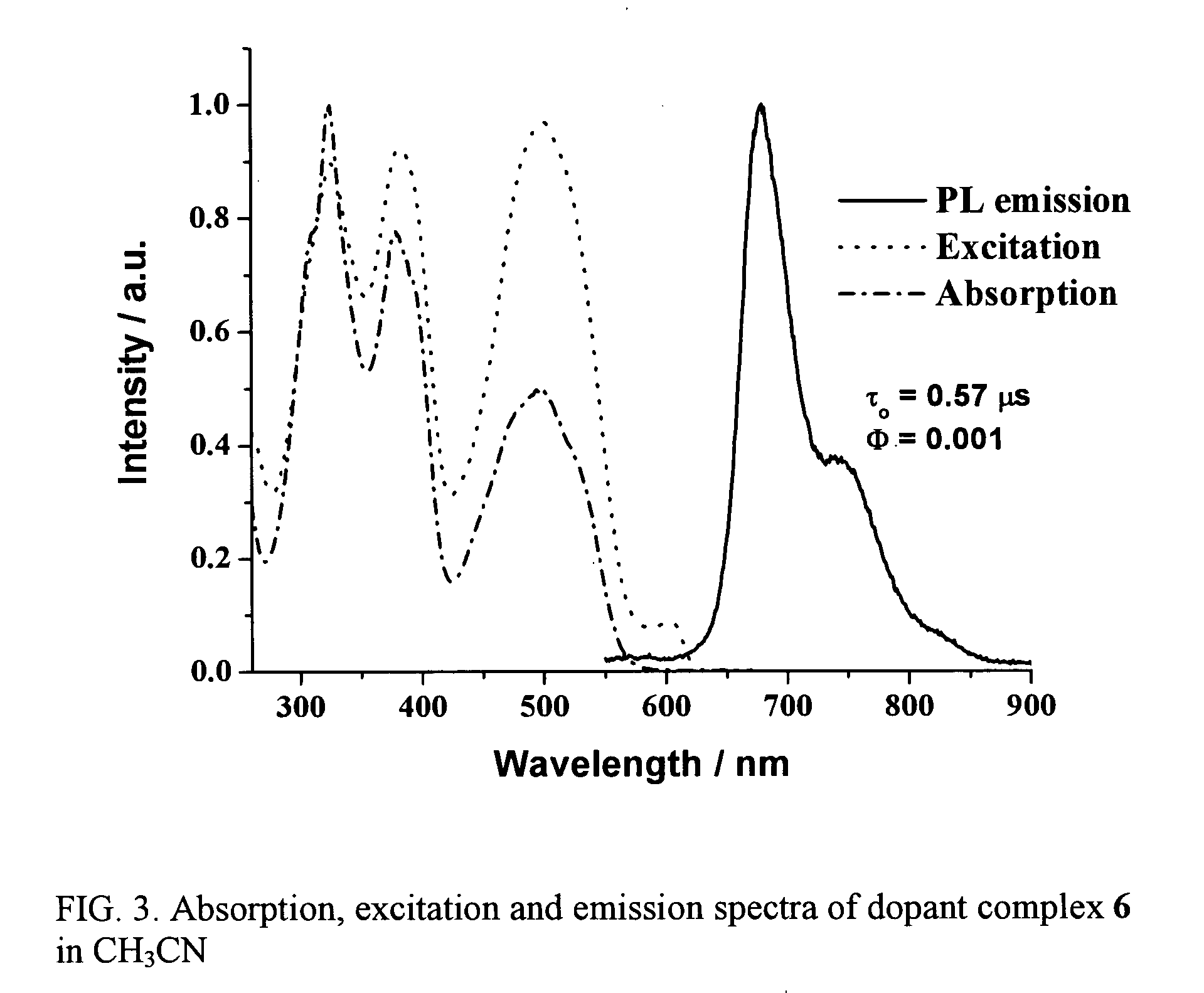
[0119] Example 2 shows the photophysical properties of non-limiting illustrative emissive materials corresponding to dopant complexes 1, 2 and 4 of the present invention. The absorption and photoluminescence properties of dopant complexes are provided in Table 3. UV / vis absorption, excitation and emission spectra of dopant complexes 1, 2 and 4 are shown in FIGS. 1 to 3 respectively. The photoluminescence (PL) spectrum is substantially independent of excitation wavelength from 300 to 450 nm. At room temperature, strong PL emissions are obtained with quantum yields (φ) up to 0.110 in CH3CN. The emission lifetimes of the dopant complexes range from 0.57 to 4.25 μs.
TABLE 3Physical characterization of dopant complexes 1, 2 and 4.Dopantλabs, sol. (nm)λem, sol.aτ (μs)bComplex[ε (10−4 dm3 mol−1cm−1)]a(nm)[Φem, sol.]1278 [1.52], 307 [1.47],566 (max),4.25 [0.097]317 [1.56], 372 [sh, 1.34],613388 [1.85], 438 [0.45],459 [sh, 0.36]2279 [1.45], 316 [1.64],563 (max),3.60 [0.110]367 [1.36], 383 [...
example 3
[0123] Example 3 illustrates a non-limiting method for preparing an OLED of the present invention. The electroluminescent devices were prepared on patterned indium-tin-oxide (ITO) glass with a sheet resistance of 20 Ω / square. The glass was cleaned sequentially in detergent solution, deionized water, ethanol and acetone. After the wet-cleaning process, the ITO glass was dried at 130° C. for 1 h and treated in UV ozone cleaner for 10 mins. In the practice of the present invention of this example, the device configuration is ITO / NPB (40 nm) / CBP:X wt. % dopant complex as illustrated in formulae (I), (II), (III) or (IV) (30 nm) / BCP (20 nm) / Alq3 (30 nm) / LiF (0.5 nm) / Al (150 nm); all of the layers were grown sequentially by thermal deposition at a deposition rate of about 0.2 Å / sec or about 5 Å / sec under a vacuum of 1×10⁻⁶ Torr.
[0124] The configuration of OLED in the present invention is schematically shown in FIG. 4. The device has multiple layers as shown. In particular, anode layer 410...
PUM
| Property | Measurement | Unit |
|---|---|---|
| Percent by mass | aaaaa | aaaaa |
| Weight | aaaaa | aaaaa |
| Color | aaaaa | aaaaa |
Abstract
Description
Claims
Application Information