

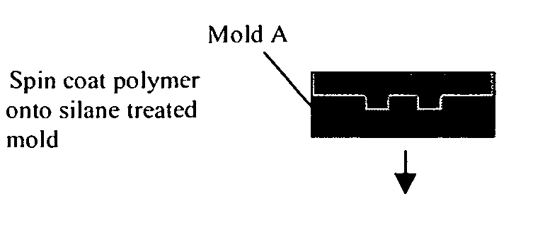
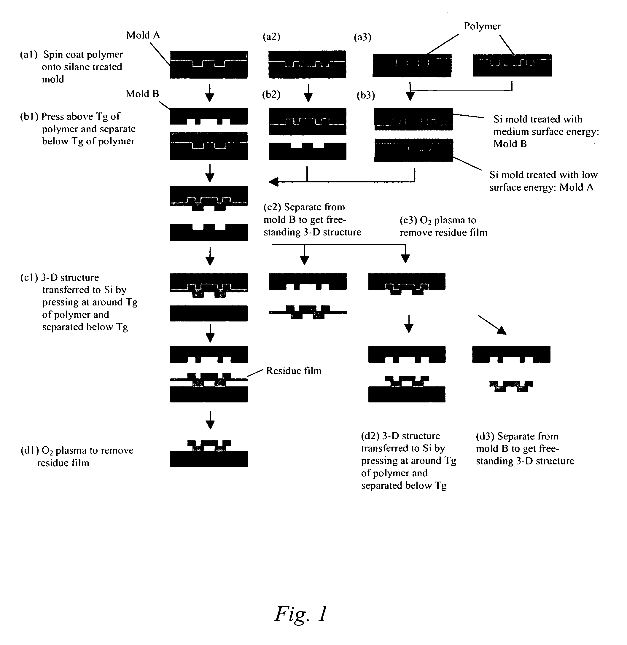
Imprinting of supported and free-standing 3-D micro- or nano-structures
a micro- or nano-structure, free-standing technology, applied in the field of micro- and nano-imprinting techniques, can solve the problems of time-consuming and labor-intensive, reducing the number of processing steps, so as to facilitate the separation of 3-d structures and eliminate the need for assembling. , the effect of fewer processing steps
- Summary
- Abstract
- Description
- Claims
- Application Information
AI Technical Summary
Benefits of technology
Problems solved by technology
Method used
Image

Examples
example 1
[0054] This Example serves to illustrate some types of 3-D micro-structures that can be formed using methods of the present invention.
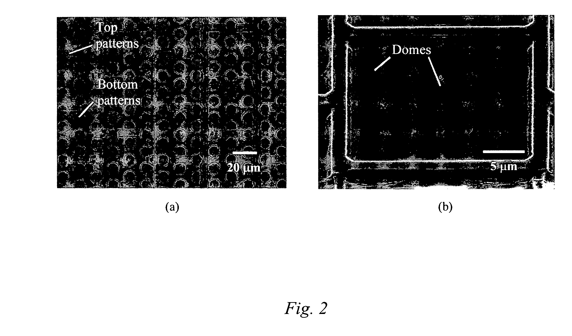
[0055]FIG. 2A depicts an optical micrograph of an imprinted 3-D structure supported on a Si substrate comprised of 20 μm wide squares on the top and 5 μm diameter circular cavities on the bottom, wherein such structures are produced by duo-mold imprinting methods of the present invention. The structures are fabricated according to the following steps: [0056] 1) Mold A is a Si mold comprising 5 μm diameter circular pillars of height 900 nm. Mold A is treated with a 20 mM silane solution (in n-heptane) of FDTS that results in a low surface energy mold. Note that in this Example, molds A and B have been pre-patterned with conventional photolithography, wherein the patterns are transferred onto the silicon with a plasma etch.
[0057] 2) Mold B is a Si mold comprising 20 μm wide squares of height 900 nm. Mold B is treated sequentially with PEDS and ODS sol...
example 2
[0060] This Example serves to illustrate an embodiment that falls within the context of sub-process B, described above.
[0061]FIG. 3 illustrates an example of an imprinted 3-D structure supported on Si. The structure comprises a grating of 700 nm pitch with a 1:1 duty cycle on the top with 3 and 5 μm wide square cavities on the bottom. The two molds that were used to form this structure comprise the following: [0062] 1) Mold A is a Si mold of 3 and 5 μm wide squares of height 250 nm. Mold A is treated with a 20 mM silane solution (in heptane) of FDTS that results in a low surface energy mold. [0063] 2) Mold B is a Si grating mold of 700 nm pitch with a 1:1 duty cycle and height 350 nm. Mold B is also treated with a 20 mM silane solution (in heptane) of FDTS that also results in a low surface energy mold.
[0064] An 8 wt. % PMMA (average MW ˜15 kg / mol) in toluene solution is spin-coated at 3000 rpm for 30 seconds onto mold B to obtain a planarized coating with a thickness of around 50...
example 3
[0067] This Example serves to better illustrate how stacked 3-D polymeric micro- or nano-structures can be formed using polymer materials of progressively lower Tg.
[0068] The duo-mold imprinting of polymers with progressively lower glass transition temperatures or of miscible polymer blends (to tune the transition from glassy behavior to viscoelastic behavior) enable the formation of stacked 3-D structures as illustrated in FIG. 4. A representative three-polymer system suitable for the formation of such stacked 3-D structures is polycarbonate (average MW ˜18.2 kg / mol, Tg˜150° C.), PMMA (average MW ˜15 kg / mol, Tg˜105° C.), and poly(t-butyl-acrylate) (average MW ˜100 kg / mol, Tg˜43° C.). In such a scenario, the first polymer to be imprinted with the duo-mold process would be polycarbonate, followed by PMMA, and finally poly(t-butyl-acrylate).
[0069] Alternatively, one could eliminate the use of progressively lower glass transition temperatures for the formation of stacked 3-D structur...
PUM
| Property | Measurement | Unit |
|---|---|---|
| Temperature | aaaaa | aaaaa |
| Structure | aaaaa | aaaaa |
| Dimension | aaaaa | aaaaa |
Abstract
Description
Claims
Application Information