Process for patterning nanocarbon material, semiconductor device, and method for manufacturing semiconductor device

a nanocarbon material and nanotechnology, applied in the field of patterning nanocarbon materials, semiconductor devices, and methods for manufacturing semiconductor devices, can solve the problems of difficult to remove catalyst layers, reduce the formation rate of carbon nanotube layers, so as to achieve the effect of convenient fabrication

Inactive Publication Date: 2005-12-01
CANON KK
View PDF6 Cites 53 Cited by
  • Summary
  • Abstract
  • Description
  • Claims
  • Application Information

AI Technical Summary

Benefits of technology

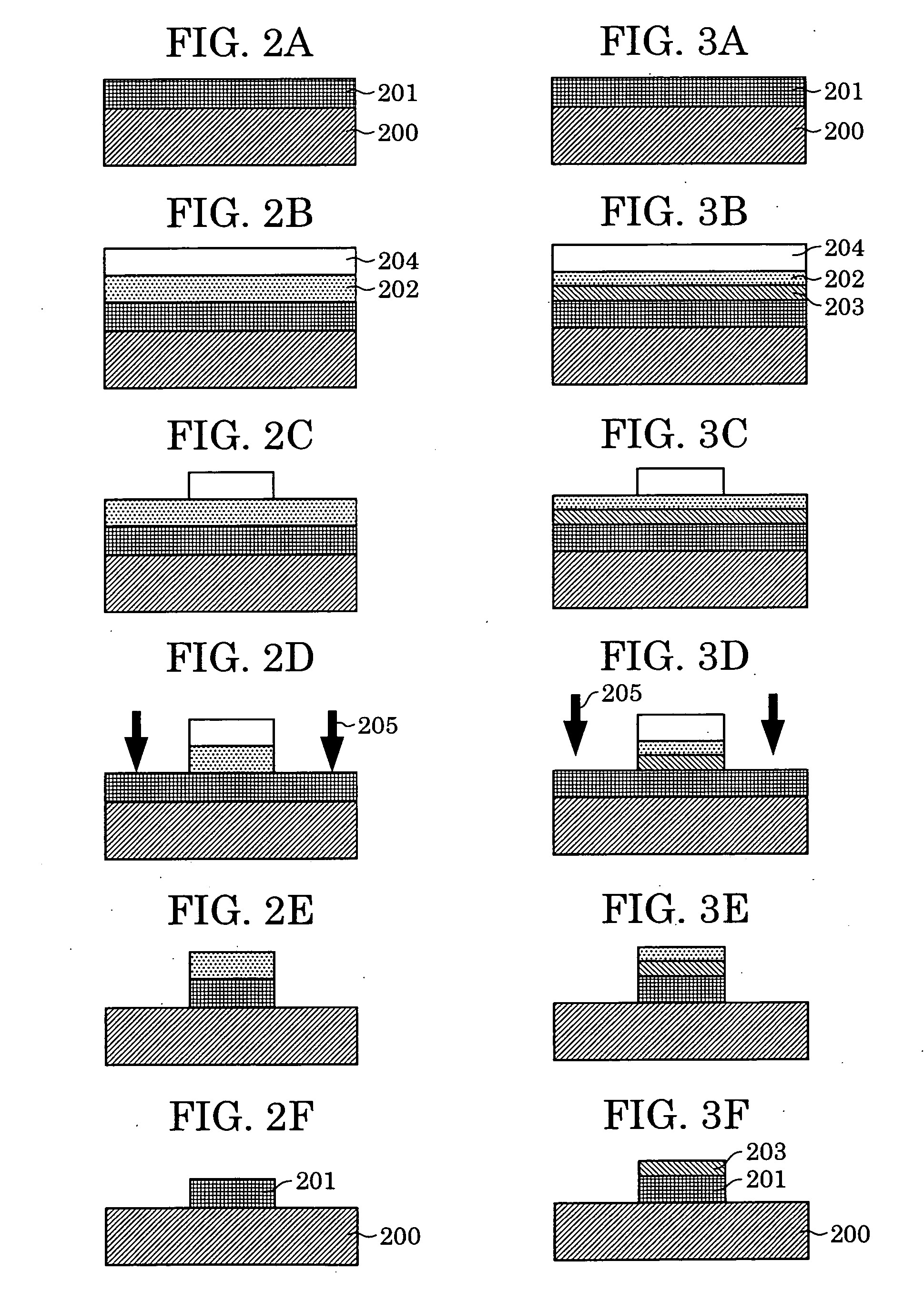
[0064] Field effect transistors including semiconductor layers containing carbon nanotubes can be readily fabricated by the procedure including the steps shown in FIG. 2A to 2F.
[0065]FIGS. 4A, 4B, and 4C are schematic sectional views showing configurations of three types of field effect transistor, fabricated by the process of the present invention, including a semiconductor layer containing carbon nanotubes. With reference to FIGS. 4A to 4C, reference numeral 300 represents substrates, reference numeral 301 represents carbon nanotube layers, reference numeral 302 represents gate insulators, reference numeral 303 represents source electrodes, reference numeral 304 represents drain electrodes, reference numeral 305 represents gate electrodes, reference numeral 306 represents insulating layers, and reference numeral 307 represents ohmic contact layers. In the field effect transistor shown in FIG. 4A, the gate electrode 305 includes a heavily doped silicon substrate.
[0066] In the process of the present invention, the carbon nanotubes are prepared in advance. Therefore, any catalyst layer containing nickel or another metal need not be formed and any high-melting point material such as molybdenum or tungsten need not be used to fabricate electrodes depending on the temperature at which the carbon nanotubes are created in contrast to known processes.
[0067] The gate electrodes 305, the source electrodes 303, and the drain electrodes 304 may contain aluminum, copper, or nickel other than a high-melting point material such as molybdenum or tungsten.
[0068] The gate insulators 302 may contain silicon dioxide, silicon nitride, tantalum oxide, or another compound and can be formed by a CVD process such as a thermal CVD process a plasma-enhanced CVD process. The substrates 300 may be made of silicon, glass, quartz, sapphire, or another material. The insulating layers 306 may be made of silicon dioxide or another compound. When the substrates 300 are made of silicon, the insulating layers 306 made of silicon dioxide can be formed by thermal oxidation. The ohmic contact layers 307 in contact with the carbon nanotubes may be made of palladium or another material.
[0069]FIG. 6 is a fragmentary sectional view showing a configuration of an FED. With reference to FIG. 6, the FED includes an insulating substrate 500 made of glass, rear electrodes 501 functioning as cathode electrodes, nanocarbon layers 502 functioning as cathodes, insulating spacers 503 functioning as partitions, fluorescent layers 504, transparent electrodes 505 functioning as anodes, a front mask 506, and a transparent front plate 507 made of glass.

Problems solved by technology

Procedure (i) has problems in that conditions for selectively growing the carbon nanotubes must be found, it is difficult to remove the catalyst layer on which the carbon nanotube layer is placed, and configurations of the devices are therefore limited.
Procedure (ii) has a problem in that the temperature at which the carbon nanotube layer is formed must be lower than the heat-resistant temperature of the resist material.
For this technique, a process for forming the mask is, however, limited to a sputtering process or a CVD process using an organometallic compound.
The technique therefore has a problem in that it is difficult to form an oxide layer for forming the mask without damaging a nanocarbon material and also has a problem in that such a nanocarbon material is deteriorated or damaged during the etching of the oxide layer.
In particular, when the oxide layer is formed on the nanocarbon material by a sputtering process, the following problems occur: damages due to argon ions, the oxidation of the nanocarbon material, and the formation of a nonuniform oxide layer.
When a silicon dioxide layer is formed by a CVD process using a compound such as tetraethoxysilane, the layer usually contains carbon and uniform layer, resistant to oxygen plasma, is therefore difficult to form.

Method used


Image

  • Process for patterning nanocarbon material, semiconductor device, and method for manufacturing semiconductor device
  • Process for patterning nanocarbon material, semiconductor device, and method for manufacturing semiconductor device
  • Process for patterning nanocarbon material, semiconductor device, and method for manufacturing semiconductor device

Examples


example 1

[0078] A wiring pattern was formed by the process of the present invention, whereby an element for measuring the resistance of a wire made of a nanocarbon material was prepared. FIGS. 7A to 7E show steps of preparing the element. With reference to FIGS. 7A to 7E, reference numeral 600 represents an insulating substrate made of Corning 7059 glass, reference numeral 601 represents electrode pads used as measurement terminals, reference numeral 602 represents a nanocarbon layer containing the carbon nanotubes, reference numeral 603 represents a mask layer (first metal layer), and reference numeral 604 represents a photoresist layer.

[0079] (1) Magnets were arranged under the rear face of the insulating substrate 600, a Permalloy mask having a negative pattern corresponding to the electrode pads 601 was placed on the front face of the insulating substrate 600, and the electrode pads 601 each including the following layers were formed on the front face of the insulating substrate 600 wit...

example 2-1

[0085] An element including a nanocarbon wire similar to that shown in FIG. 7E was prepared by the same procedure as that described in Example 1 except that a mask layer 603 of this element included no Cu sub-layer nor Zn sub-layer, but did contain Zn, and had a thickness of 200 nm.

example 2-2

[0086] An element having the same configuration as that described in Example 2-1 was prepared and a mask layer 603 of this element was then etched off with ammonia water.


PUM

PropertyMeasurementUnit
sizeaaaaaaaaaa
temperatureaaaaaaaaaa

Abstract

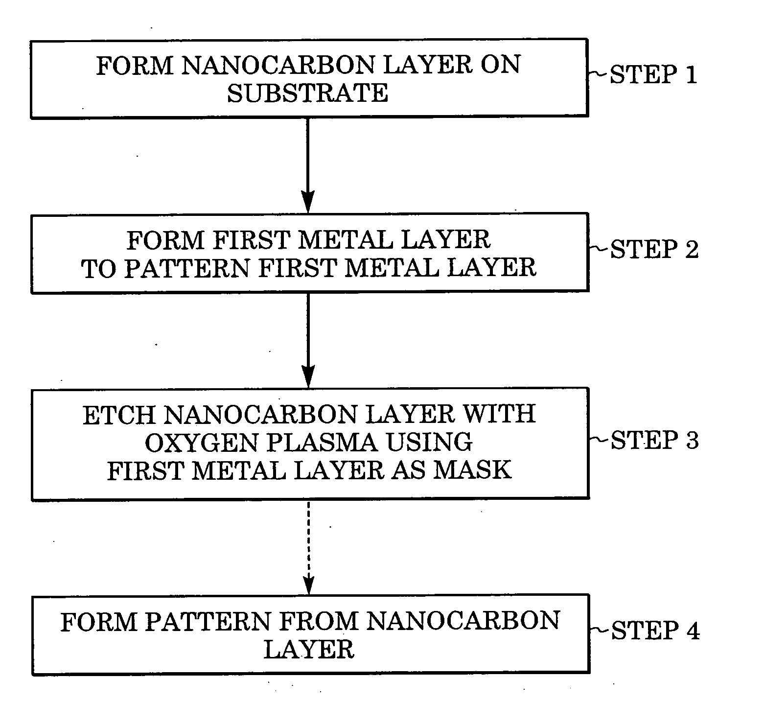
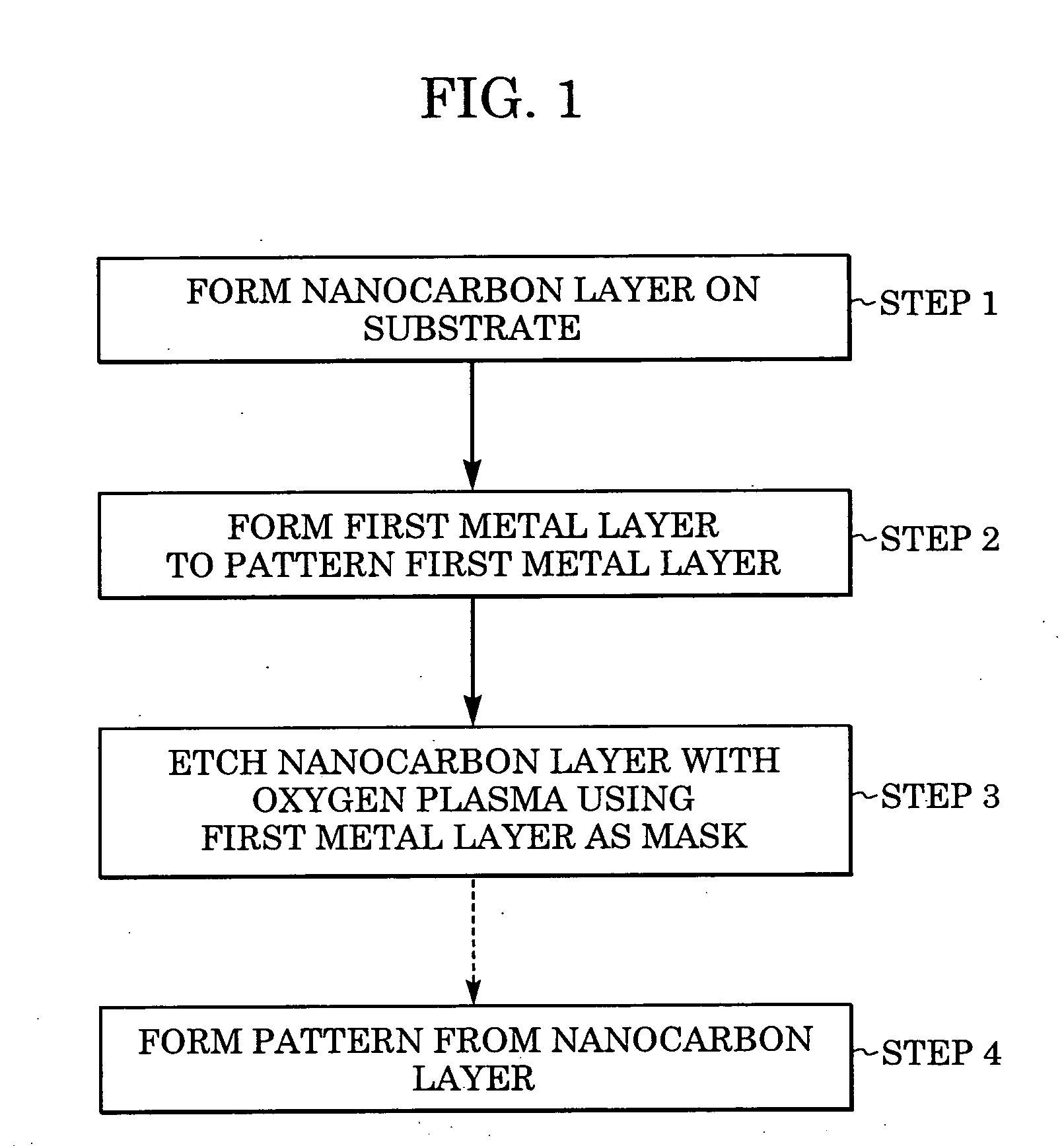
A process for patterning a nanocarbon material includes a step of forming a nanocarbon layer on a substrate; a step of forming a first metal layer on the nanocarbon layer to pattern the first metal layer, the first metal layer containing at least one selected from the group consisting of zinc, tin, indium, aluminum, and titanium; and a step of etching the nanocarbon layer with oxygen plasma using the first metal layer as a positive pattern. Also, a method for manufacturing a semiconductor device including a semiconductor layer containing a nanocarbon material includes a step of patterning a nanocarbon material by the above process; and, a semiconductor device containing a nanocarbon material includes a semiconductor layer including a nanocarbon sub-layer patterned by the process.

Description

BACKGROUND OF THE INVENTION [0001] 1. Field of the Invention [0002] The present invention relates to a process for patterning a nanocarbon material, a semiconductor device including a patterned nanocarbon material, and a method for manufacturing such a semiconductor device. [0003] 2. Description of the Related Art [0004] Since H. W. Kroto, R. E. Smalley, and R. F. Curl discovered soccer ball-shaped molecules, called fullerenes, consisting of 60 carbon atoms in 1985 and S. Iijima discovered tubular structures, called carbon nanotubes, including rolled graphene sheets in 1991, various applications of these materials have been actively investigated. [0005] The carbon nanotubes have excellent field emission properties, high heat conductivity, low weight, and high density; intercalate or deintercalate lithium ions due to electrochemical reaction; act as conductors or semiconductors depending on their chirality; and provide high-density currents. Therefore, carbon nanotubes have been inve...

Claims


Application Information

Patent Timeline
Patent Type & Authority Applications(United States)
IPC IPC(8): B29C45/14B41F13/18B29C45/26B29C45/76B29K75/00B29L31/32B41F35/06H01J9/02H01L21/302H01L21/3213H01L51/00H01L51/05
CPCB82Y10/00B82Y30/00H01J9/025H01J2201/30469H01L51/0545H01L51/0018H01L51/0048H01L51/0525H01L21/32139Y10S977/842H10K71/233H10K85/221H10K10/472H10K10/466
Inventor KAWAKAMI, SOICHIRO
Owner CANON KK
Why Eureka
Try Eureka