

Semiconductor device fabricating method
a technology of semiconductor devices and fabrication methods, applied in the direction of semiconductor devices, basic electric elements, electrical equipment, etc., can solve the problems of limited operation speed of semiconductor devices as a whole, limited nanonization, and difficult technology of nanonization, etc., to achieve the effect of improving the operation speed of p-transistor
- Summary
- Abstract
- Description
- Claims
- Application Information
AI Technical Summary
Benefits of technology
Problems solved by technology
Method used
Image

Examples
first embodiment
A First Embodiment
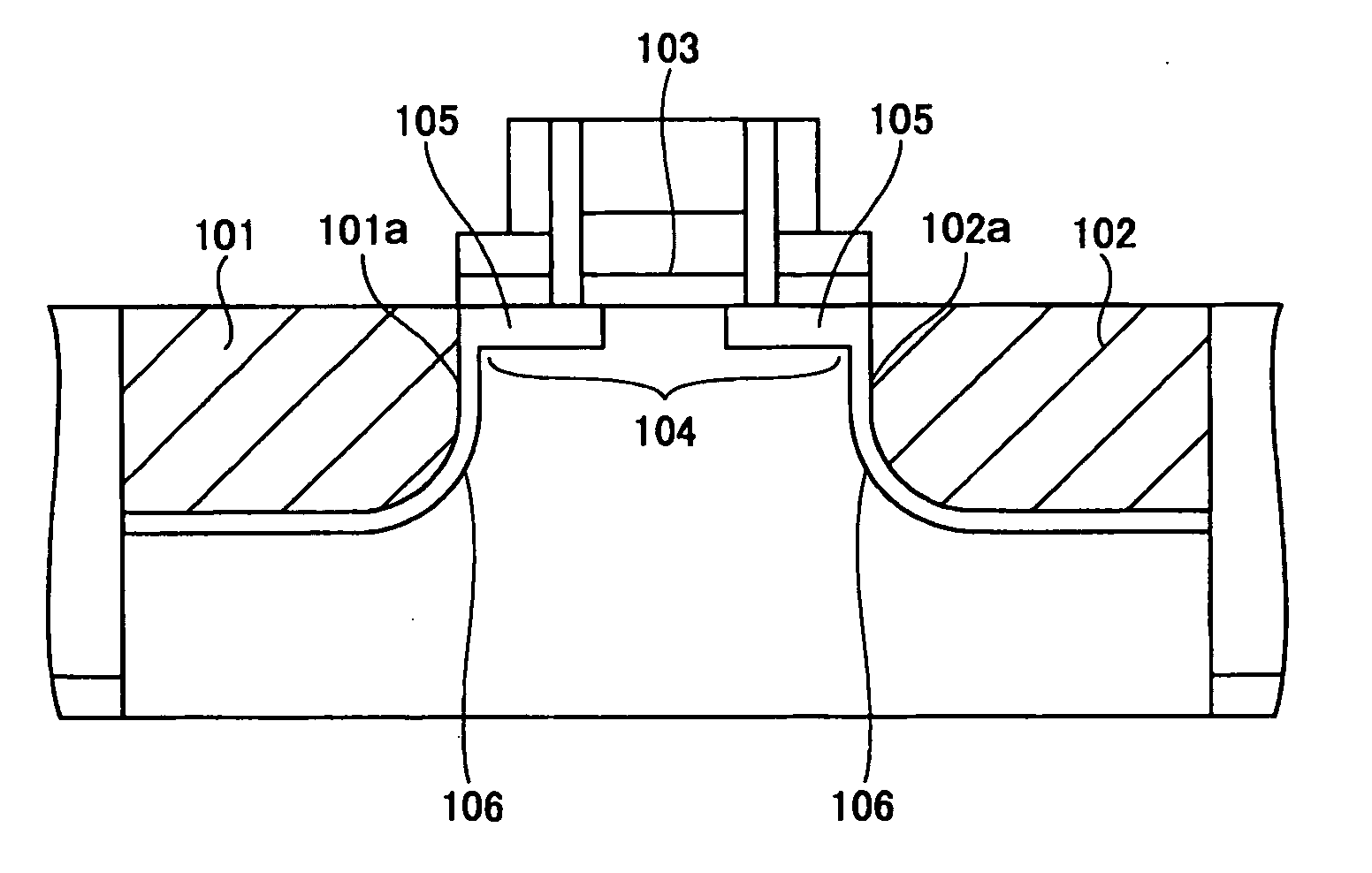
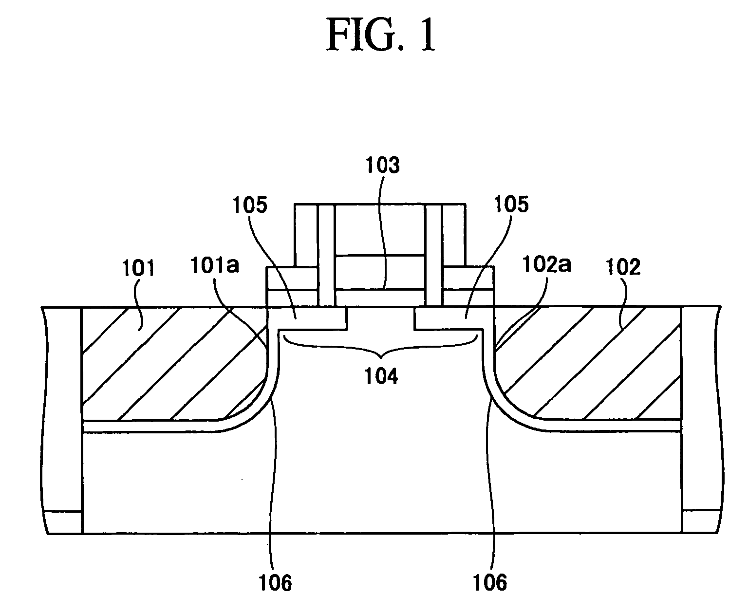
[0048] A semiconductor device fabricating method according to a first embodiment of the present invention will be explained with reference to FIGS. 2 to 17. FIG. 2 is a sectional view of a semiconductor device fabricated by the semiconductor device fabricating method according to the first embodiment of the present invention. FIGS. 3 to 17 are sectional view of the semiconductor device in the steps of the semiconductor fabricating method according to the present embodiment, which illustrate the method.
[0049] With reference to FIG. 2, the semiconductor device 10 comprises a p-MOS transistor 13a and an n-MOS transistor 13b spaced from each other by a device isolation region 12. In the p-MOS transistor 13a, compressive stress applying portions 20 of, e.g., SiGe are formed outward from the surfaces of the silicon substrate 11 in contact with a third sidewall insulation film 19 formed on both side surfaces of a gate layer structure 18 formed of a gate insulation film 1...
second embodiment
A Second Embodiment
[0092] The semiconductor device fabricating method according to a second embodiment of the present embodiment will be explained with reference to FIGS. 18 to 22. FIGS. 18 to 22 are sectional views of the semiconductor device in the steps of the semiconductor device fabricating method according to the second embodiment of the present invention, which illustrate the method. The parts of the semiconductor device corresponding to the parts explained above are indicated by the same reference numbers not to repeat their explanation.
[0093] The second embodiment of the present invention is characterized in that in etching the trenches for the compressive stress applying portions to be formed in, a mask which is different fro that of the first embodiment is used.
[0094] First, in the step of FIG. 18, the same steps of FIGS. 3 to 6 of the first embodiment are performed to form the structure with a silicon oxide film 34-1 and a silicon nitride film 35-1 deposited, covering ...
third embodiment
A Third Embodiment
[0109] The semiconductor device fabricating method according to a third embodiment of the present invention will be explained with reference to FIGS. 23 to 29. FIGS. 23 to 29 are sectional view of a semiconductor device in the steps of the semiconductor fabricating method according to the third embodiment, which illustrate the method. The same part as the parts described above are represented by the same reference numbers not to repeat their explanation.
[0110] The third embodiment of the present invention is different from the first embodiment I that the shallow junction regions are double-stepped.
[0111] The semiconductor device fabricating method according to the third embodiment is the same as the first embodiment in the steps of FIGS. 2 to 14. That is, in the step of FIG. 13, in an n-MOS region 30b, an n-impurity is implanted in a silicon substrate 11 on both sides of a gate layer structure 18 by ion implantation with the gate layer structure as the mask to fo...
PUM
 Abstract
Description
Claims
Application Information