Image sensor and method for manufacturing the same

a technology of image sensor and manufacturing method, which is applied in the direction of instruments, semiconductor/solid-state device details, radiation control devices, etc., can solve the problems of limiting device sensitivity, affecting information presented on the display, and reducing the amount of light available in the light-receiving region of the device, so as to increase the efficiency of photon transfer and increase efficiency

Active Publication Date: 2005-12-29
SAMSUNG ELECTRONICS CO LTD
View PDF4 Cites 75 Cited by
  • Summary
  • Abstract
  • Description
  • Claims
  • Application Information

AI Technical Summary

Benefits of technology

[0010] The present invention is directed to a solid state imaging device, and a method of manufacture thereof, which increases the efficiency of the transfer of available photons to the photo-receiving elements beyond that which is currently available. The en...

Problems solved by technology

If the photon count being transmitted to the photo-reception elements is less than a threshold amount, the information presented on the display is adversely affected.
With these goals in mind, the amount of light available at the light-receiving region of the device has been reduced, due to the reduced device size, thereby limiting device sensitivity.
Howeve...

Method used


Image

  • Image sensor and method for manufacturing the same
  • Image sensor and method for manufacturing the same
  • Image sensor and method for manufacturing the same

Examples


first embodiment

[0058]FIGS. 6A-6F are cross-sectional views of a process for forming an image sensor in accordance with the present invention. In the drawings of FIGS. 6A to 6F, a CCD device image sensor is depicted; however, the principles of the present invention apply equally well to CIS-type image sensors, and other forms of image sensors, and methods of fabrication thereof,

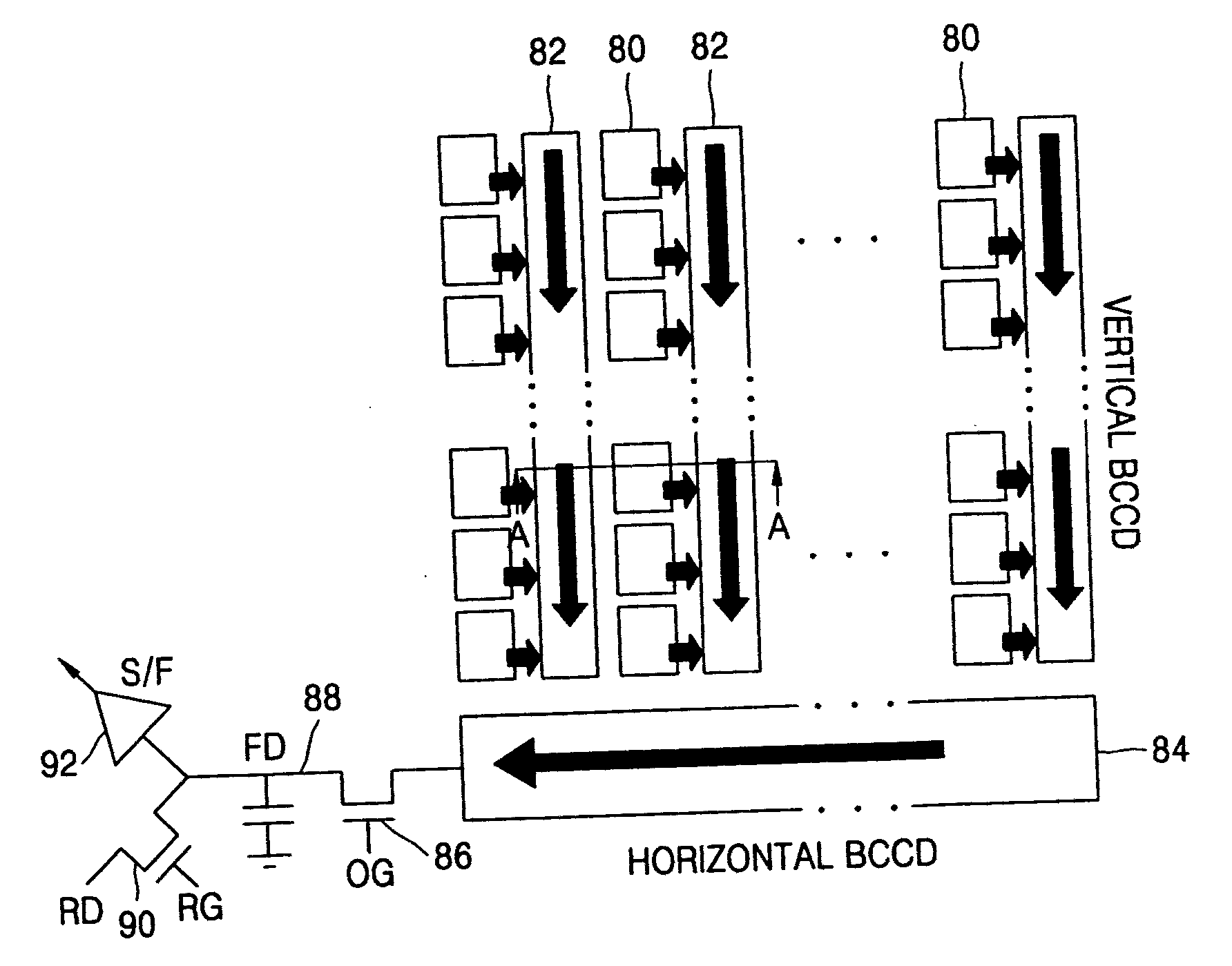
[0059]FIG. 6A is a cross-sectional view of the CCD device of FIG. 4 taken along section line A-A. With reference to FIG. 6A, a p type well 101 is formed in a region of a semiconductor substrate 100, for example a silicon-based substrate. The p type well 101 is formed by implanting boron B at an energy level of 3 MeV, and a dopant concentration of 2E11 / cm2. A photon-receiving region 102 is formed in the p type well 101 by implanting arsenic As at an energy level of 800 eV, and a dopant concentration of 2E11 / cm2. A p+ type channel stop region 110 is formed at a first side of the photon-receiving region 102 by implanting a p ty...

second embodiment

[0070]FIGS. 7A-7E are cross-sectional views of a process for forming an image sensor in accordance with the present invention.

[0071]FIG. 7A is a cross-sectional view of the CCD device of FIG. 4 taken along section line A-A in accordance with a second embodiment of the present invention. In the same manner as the embodiment shown in FIG. 6E, the solid state imaging device of FIG. 7A includes a first silicon dioxide layer 131 and a first silicon oxynitride layer 133. However, prior to patterning of the silicon oxynitride layer 133 as shown in FIG. 6F of the first embodiment, the present second embodiment includes a second silicon dioxide layer 141 and a silicon nitride layer 143 that are sequentially formed on the silicon oxynitride layer 133. Therefore, in this embodiment, the anti-reflection layer 140 includes the first silicon dioxide layer 131, the silicon oxynitride layer 133, the second silicon dioxide layer 141, and the silicon nitride layer 143, applied sequentially. As in the...

third embodiment

[0077]FIGS. 8A-8D are cross-sectional views of a process for forming an image sensor in accordance with the present invention

[0078]FIG. 8A is a cross-sectional illustration of a solid state imaging device having a multiple layered anti-reflection layer 140 applied in a manner similar to that described above with reference to FIG. 7A. In this embodiment, a hard mask 200, for example comprising silicon dioxide, is layered on the anti-reflection layer 140.

[0079] Referring to FIG. 8B, the hard mask 200 is patterned to form a patterned hard mask 200′ according to conventional photolithographic techniques in a region above the photon-receiving region 102 as shown.

[0080] Referring to FIG. 8C, the silicon nitride layer 143′ is etched in a wet etch process using phosphoric acid (H3PO4) as an etch solution.

[0081] Referring to FIG. 8D, the second silicon dioxide layer 141′ and the silicon oxynitride layer 133′ are subsequently etched using a wet etching process utilizing hydrofluoric acid (...


PUM


Abstract

In a solid state imaging device, and a method of manufacture thereof, the efficiency of the transfer of available photons to the photo-receiving elements is increased beyond that which is currently available. Enhanced anti-reflection layer configurations, and methods of manufacture thereof, are provided that allow for such increased efficiency. They are applicable to contemporary imaging devices, such as charge-coupled devices (CCDs) and CMOS image sensors (CISs). In one embodiment, a photosensitive device is formed in a semiconductor substrate. The photosensitive device includes a photosensitive region. An anti-reflection layer comprising silicon oxynitride is formed on the photosensitive region. The silicon oxynitride layer is heat treated to increase a refractive index of the silicon oxynitride layer, and to thereby decrease reflectivity of incident light at the junction of the photosensitive region.

Description

RELATED APPLICATIONS [0001] This application claims the benefit of Korean Patent Application No. 2004-49001, filed on Jun. 28, 2004, the disclosure of which is hereby incorporated herein by reference in its entirety. BACKGROUND OF THE INVENTION [0002] Solid-state imaging devices enjoy widespread use in contemporary imaging systems. Popular solid-state imaging devices include charge-coupled devices (CCD) and CMOS image sensors (CIS). Such devices are commonly employed in digital still cameras, digital video cameras, cellular telephones, and security systems. [0003] The solid state imaging device converts transmitted light in the form of photon energy to electrical signals, and the electrical signals are converted to information that can be presented on display devices or otherwise processed by a computer system. CCD and CIS imaging devices include photo-reception elements such as photodiodes. Therefore, a significant factor in the efficiency and efficacy of such devices is the abilit...

Claims


Application Information

Patent Timeline
IPC IPC(8): G03F7/00G03F7/09H01L21/314H01L27/146H01L27/148
CPCG03F7/091H01L21/3144H01L21/3145H01L27/14609H01L27/14843H01L27/14627H01L27/14643H01L27/14685H01L27/1462H01L21/0214H01L27/146
Inventor MOON, CHANG ROK
Owner SAMSUNG ELECTRONICS CO LTD
Why Eureka
Try Eureka