Microneedle array device and its fabrication method

a technology of microneedle array and fabrication method, which is applied in the field of microneedle array structure, can solve the problems of high cost, low yield rate, and complicated fabrication process of si substrate, and achieve the effect of low cost and simple process

Inactive Publication Date: 2006-01-19
IND TECH RES INST
View PDF8 Cites 88 Cited by
  • Summary
  • Abstract
  • Description
  • Claims
  • Application Information

AI Technical Summary

Benefits of technology

[0011] According to the present invention, there are several techniques to be used in step (1) of forming a plurality of concave areas, including etching, X-ray photo-etching, ultra-violet etching, ion beam etching and excimer laser micromachining. Step (4) of the method further includes the following substeps: (4a) coating a layer of metal on the outer surface of the polymer hollow microneedle array mold and the light transmission material to form a microneedle array; and (4b) removing the polymer hollow microneedle array mold from the microneedle array. In step (4), the techniques for coating metal to the surface of the polymer hollow microneedle ar

Problems solved by technology

However, the fabrication process of using Si substrate is more complicated, as disclosed in WO0217985, and requires many steps of wet/dry etching and thin film deposition.
As it takes a longer time to fabricate, the yield rate is low and the cost is high.
This type of design limits the width of the flow channel and the flexibility of the needle.
The restriction of low needle density further causes the problem of insufficient sampling.
In addition, the Si substrate microneedles are brittle and break easily.
However, the method req

Method used


Image

  • Microneedle array device and its fabrication method
  • Microneedle array device and its fabrication method
  • Microneedle array device and its fabrication method

Examples


first embodiment

[0033]FIGS. 7A-7J shows the fabrication method of the present invention. First, a substrate is provided, which including a plurality of concave areas on the surface. According to the present invention, there are several techniques for forming a plurality of concave areas, including etching, X-ray photo-etching, ultra-violet etching, ion beam etching and excimer laser micromaching. The present embodiment uses an anisotropic wet etching for explanation.

[0034] As shown in FIG. 7A, a single crystal silicon with a grainorientation [1,0,0] is used as a substrate 700, and a protective layer 702 is deposited on the surface. Protective layer 702 can be made of Si3N4. The wet etching areas 705 are defined, as shown in FIG. 7B, followed by wet etching. The solution commonly used in silicon anisotropic wet etching includes potassium hydroxide (KOH) and Tetra-methyl-ammonium hydroxide (TMAH). After etching the silicon, a plurality of concave areas 710 are formed. Each concave area 710 has two sl...

second embodiment

[0045]FIGS. 11A-11K show the fabrication method of the present invention.

[0046] The fabrication method of the second embodiment is similar to that of first embodiment. The only difference is in the exposure and development step. Because the second embodiment has a reservoir layer 91 in the structure, the second embodiment requires an additional exposure than the first embodiment. During the second exposure, a corresponding patterned mask 750a is used to define reservoir layer 91 and the shape of reservoir units 93 within. By adjusting the exposure dosage to control the depth “a” of the reservoir layer, the result of this step is to obtain a polymer hollow microneedle array mold 160. The remaining steps of the fabrication are identical to those in FIG. 7A-7J.

third embodiment

[0047]FIGS. 12A-12L show the fabrication method of the present invention.

[0048] The fabrication method of the third embodiment is also similar to that of first embodiment The only difference is still in the exposure and development step. Similarly, because the third embodiment has two more reservoir layers 101 in the structure, the third embodiment requires two additional exposures than the first embodiment. During the second and third exposures, a corresponding patterned mask 750a, 750b is used to define, respectively, each reservoir layer 101 and the shape of reservoir units 103 within. By adjusting the exposure dosage to control the depths “a” and “b” of the reservoir layers, the result of this step is to obtain a polymer hollow microneedle array mold 260. Therefore, according to the present invention, the first exposure is to form the shape and the structure of the microneedles, and the second and subsequent exposures are for forming the shape and the structure of the reservoir ...


PUM

PropertyMeasurementUnit
Lengthaaaaaaaaaa
Lengthaaaaaaaaaa
Heightaaaaaaaaaa

Abstract

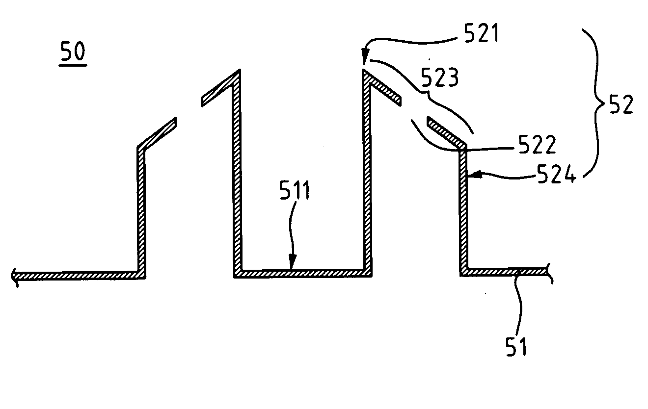
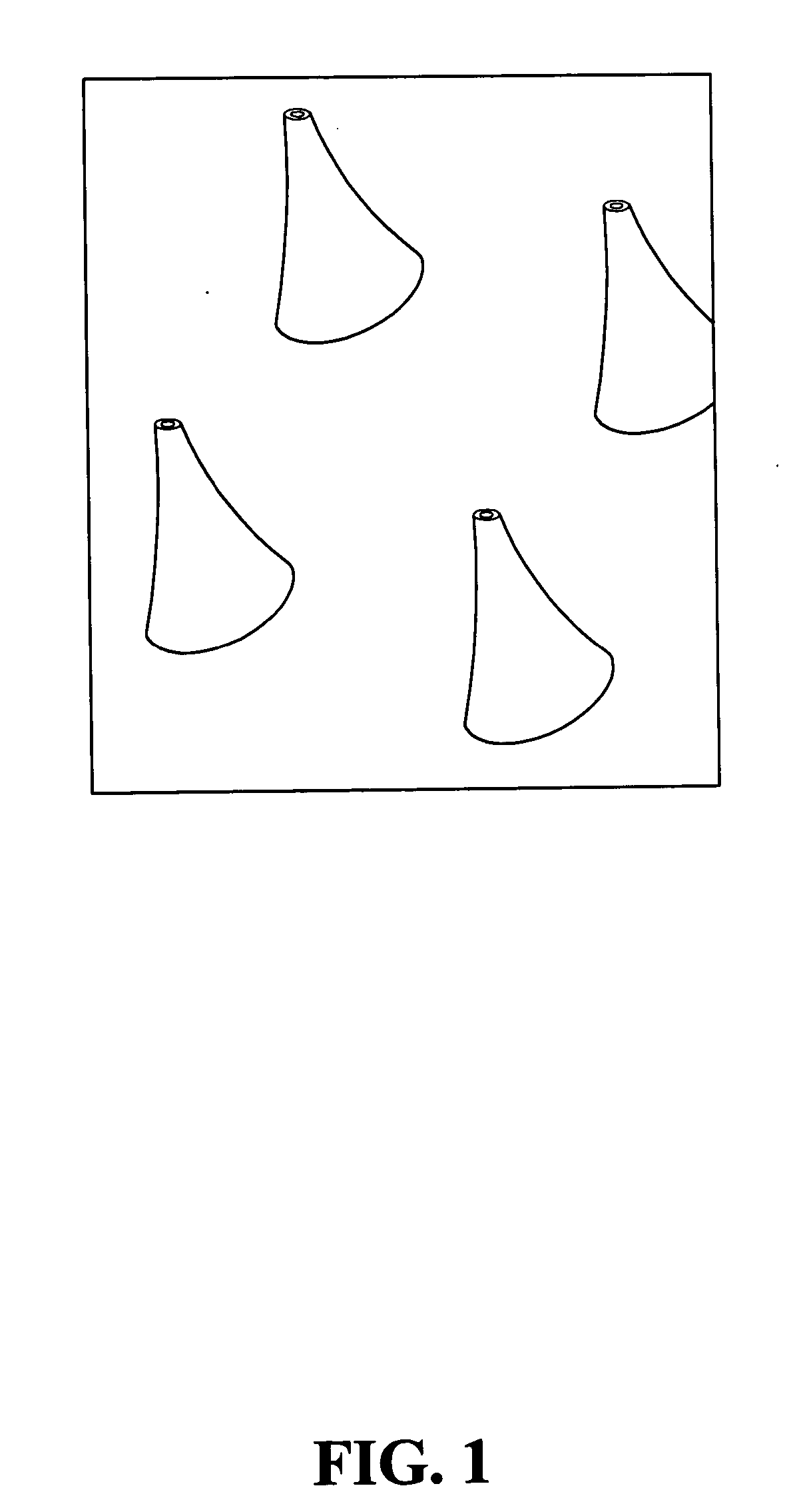
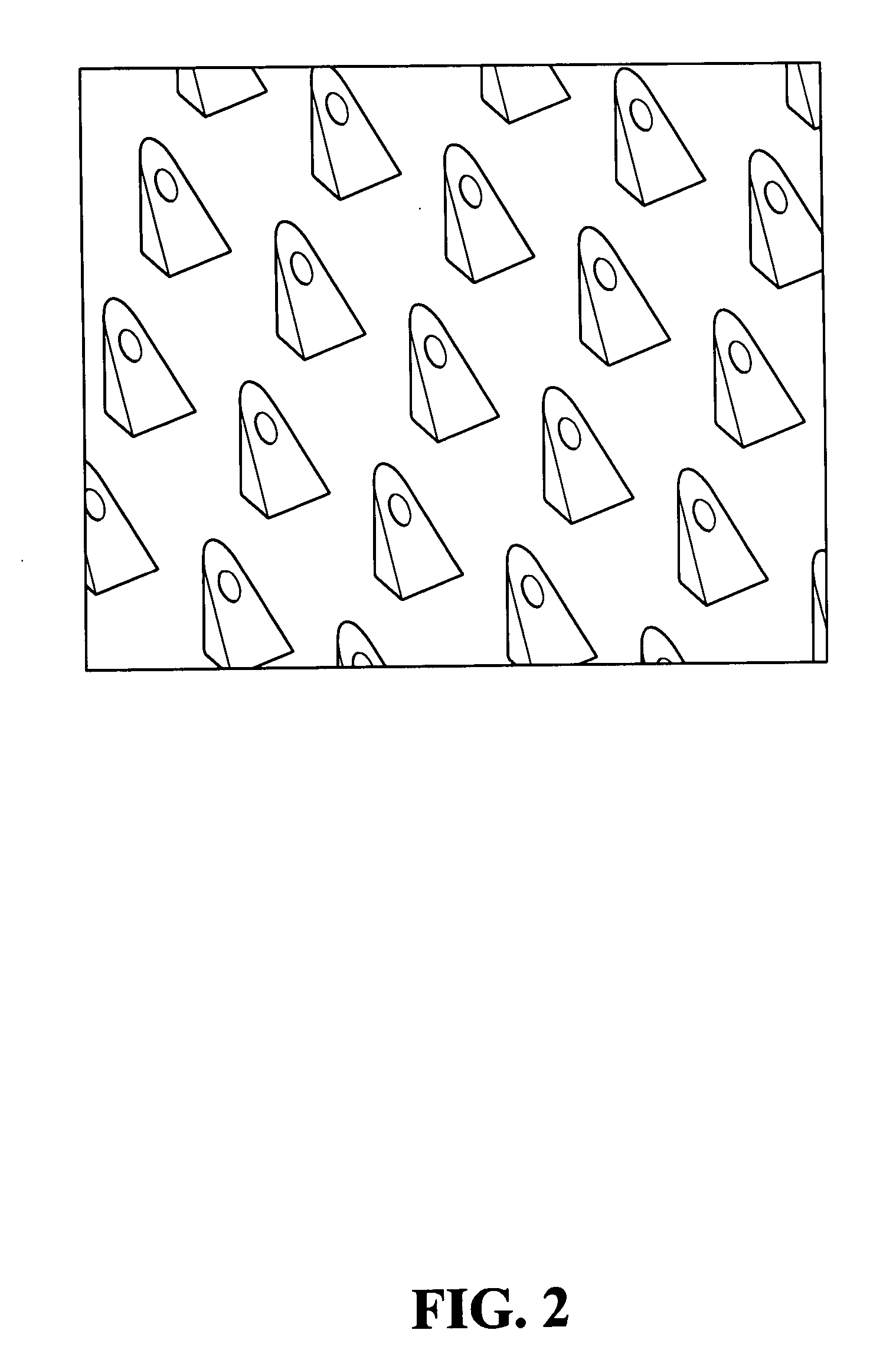
A microneedle array device and its fabrication method are provided. The microneedle array device comprises a supporting pad and plural of microneedles. Each microneedle has a top portion with a via thereon, thereby the microfluid may flow in or out. The intersection between the top portion and the inner tube of a microneedle forms a convex needle structure, and is almost perpendicular to the upper surface. For each microneedle, a hollow closed tube is formed between the top portion and the supporting pad. The fabrication method uses the substrates with high transmittance and plural of convex area thereon as the upper and lower caps, and applies a photolithography process to fabricate a microneedle array mold. It then sputters or electroplates metal material on the mold. The microneedle array is formed after having taken off the mold. It is a simple fabrication process.

Description

FIELD OF THE INVENTION [0001] The present invention generally relates to a microneedle array structure, and more specifically to a microneedle array device, and a method of forming the same. BACKGROUND OF THE INVENTION [0002] The current microneedle array may be made of silicon (Si substrate), metal or polymer. The manufacturing methods of Si substrate microneedle array can further be categorized as using wet etching or dry etching. The manufacturing process of metal microneedle array can further be categorized as using electroplating or deposition. The manufacturing process of polymer microneedle array can be further categorized as using molding or photolithography. [0003] Among the methods of microneedle array, the most widely adopted is using Si substrate to fabricate the hollow needles or mold. However, the fabrication process of using Si substrate is more complicated, as disclosed in WO0217985, and requires many steps of wet / dry etching and thin film deposition. As it takes a l...

Claims


Application Information

Patent Timeline
IPC IPC(8): A61B17/20
CPCA61B17/205B81B2201/055B81C1/00111A61M37/0015Y10T29/49982Y10T29/302Y10T29/308Y10T29/304A61M2037/0053
Inventor KUO, SHIH-CHICHOU, YU-KON
Owner IND TECH RES INST
Why Eureka
Try Eureka