Semiconductor devices with inductors

a technology of inductors and semiconductor devices, which is applied in the direction of automatic frequency control, automatic frequency control details, and semiconductor/solid-state device details, etc., can solve the problems of inability to use a semiconductor device produced by a common method, output of unwanted noise, and circuit malfunction

Active Publication Date: 2006-02-23
RENESAS ELECTRONICS CORP
View PDF14 Cites 32 Cited by
  • Summary
  • Abstract
  • Description
  • Claims
  • Application Information

AI Technical Summary

Benefits of technology

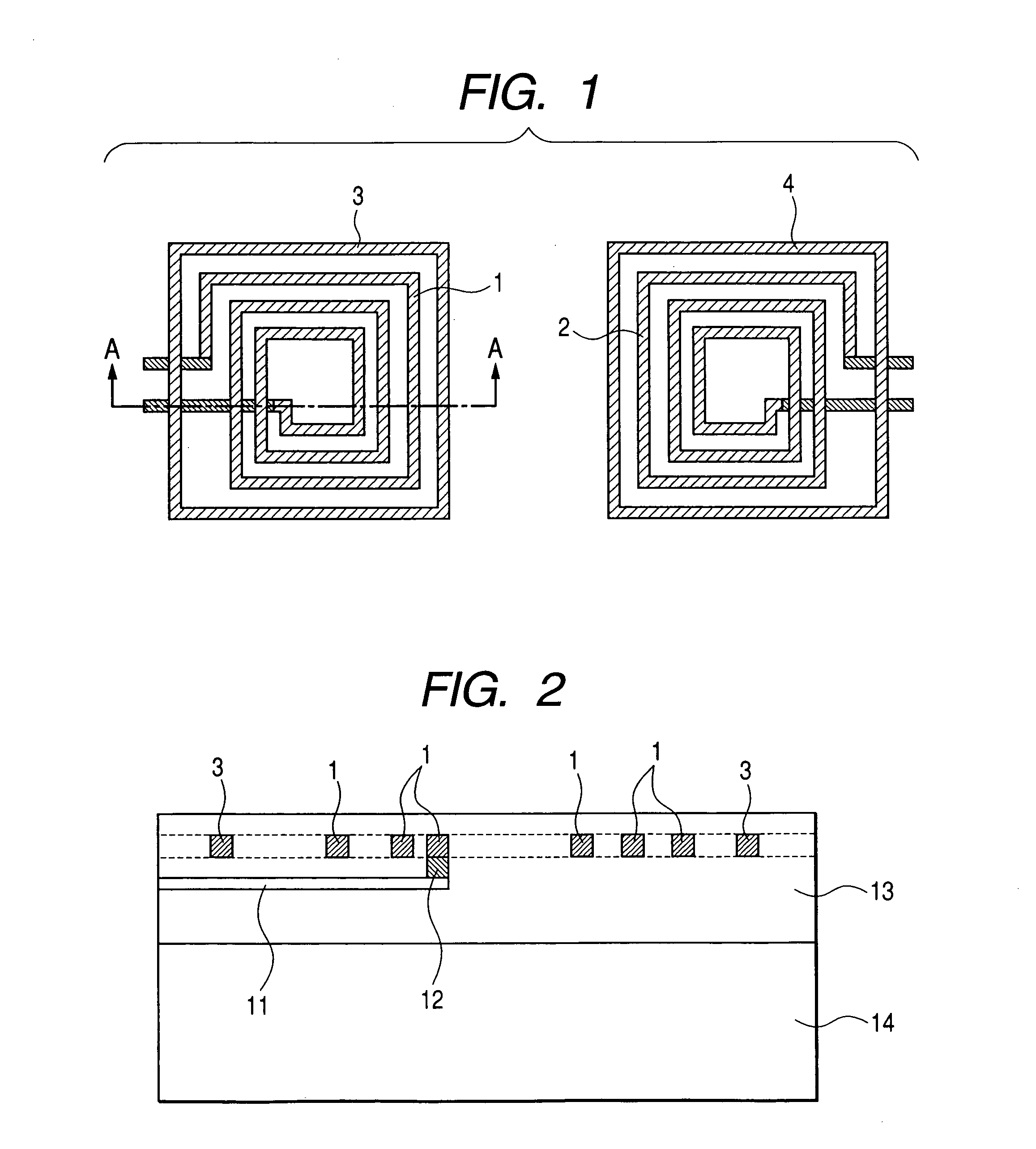
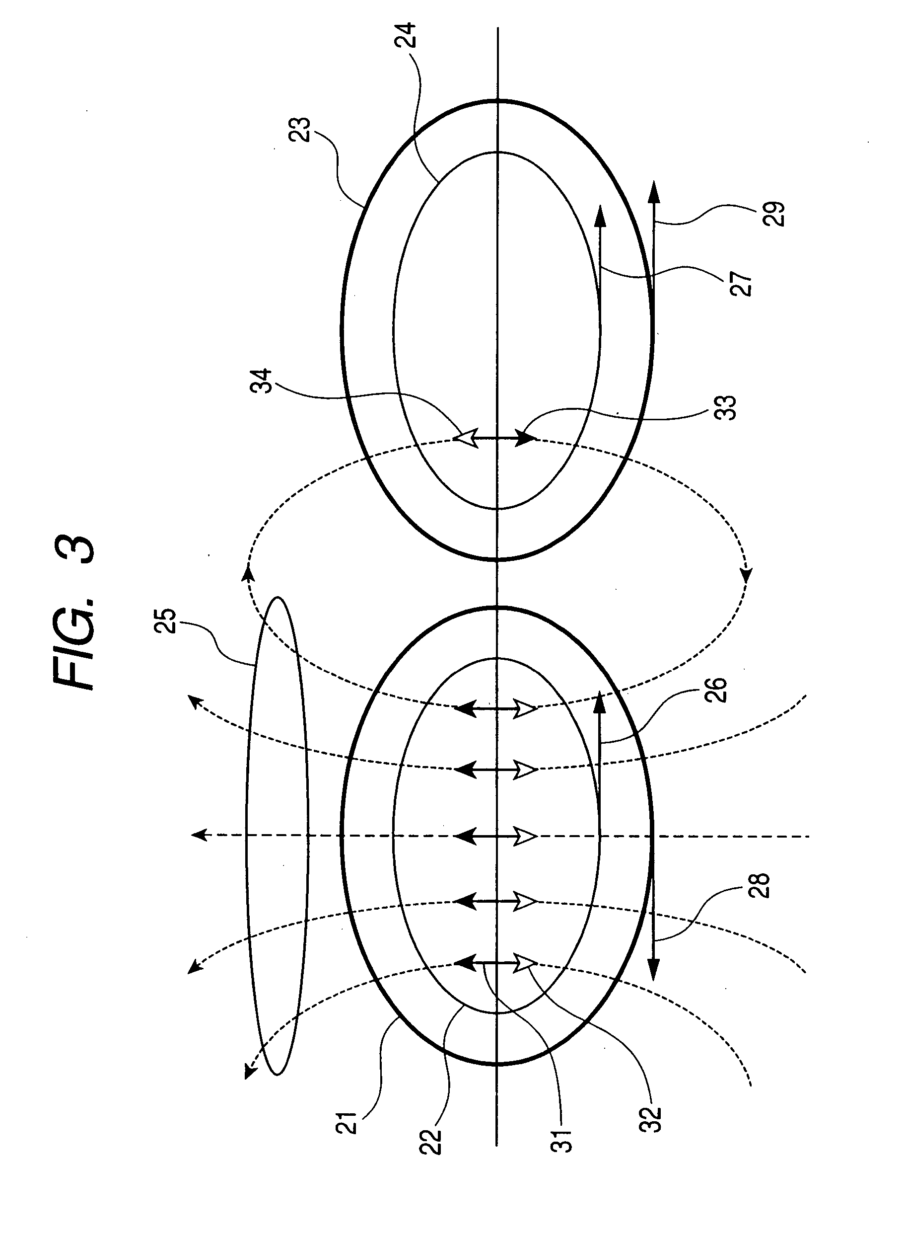
[0019] As mentioned later, the enclosure around the respective inductors by the closed loop wire attenuates interference caused by mutual inductance. The above first through third circuits respectively are realized as a modulator circuit, a demodulator circuit and a local oscillator respectively, which circuits are made into high-frequency

Problems solved by technology

Although an inductor, which is one of the fundamental passive elements of a circuit, is used widely for an oscillator, a filter, a matching circuit, a transformer and so forth, it is scarcely used for a semiconductor device produced by a common method because of its difficulty with gaining larger inductance.
Thus, it results in the inductors and the circuits being disposed nearby therein so that such problems occur as signals interference between inductors and interference between inductors and wires.
The occurrence of such signals interference within the semiconductor device invites the malfunction of the circuits, the output of unwanted noise and the deterioration of the input sensitivity.
Thus, when there is interference between the local oscillat

Method used


Image

  • Semiconductor devices with inductors
  • Semiconductor devices with inductors
  • Semiconductor devices with inductors

Examples


first embodiment

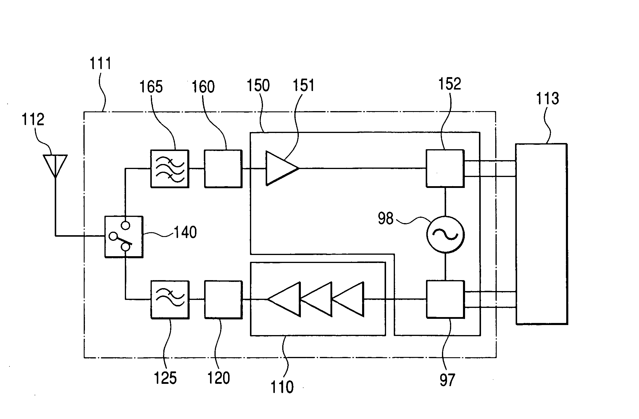
[0053]FIG. 10 shows the first embodiment of the invention. In this embodiment, inductors provided with wires for reducing the inductive coupling in the modulator circuit 97 are exemplified. In the drawing, reference numerals 61 and 62 respectively indicate inductors, reference numerals 63 indicates a wire for reducing the inductive coupling forming a closed loop wire, reference numeral 64 indicates a modulator, reference numerals 66a through 66d respectively indicate buffers, reference numerals 67a and 67b respectively indicate base band signal inputs, reference numerals 68a and 68b respectively indicate carrier wave inputs, reference numeral 69a and 69b indicate RF signal outputs and reference numeral 70 indicates a capacitor. Base band signals orthogonal to each other are input to the base band signal inputs 67a and 67b. The respective orthogonal base band signals are of bipolar differential signals whose polarity is inversed to each other. Carrier waves (local oscillation signals...

second embodiment

[0057]FIG. 11 shows the second embodiment of the invention. In this embodiment, inductors provided with a wire for reducing the inductive coupling in the local oscillator 98 are exemplified. In the drawing, reference numerals 71, 72, 73, 74, 75, 76, 77, 78, 79, 80 and 81 respectively indicate an inductor acting as a choke coil, a wire for reducing the inductive coupling forming a closed loop wire, a resonance inductor of an oscillator, a varactor diode of variable capacity, a capacitor, a transistor, a variable current source to define the operational current of the transistor, a power source voltage to the transistor 76, a frequency controller, an oscillator output and a ground. In this embodiment, the inductor (i.e. choke coil) 71 takes the interfered side.

[0058] An oscillation frequency is defined by the frequency of a resonance circuit including the indicators 73, varactor diodes 74 and capacitors 75. When control voltage is provided to the frequency controller 79, the bias vol...

third embodiment

[0061]FIG. 12 shows the third embodiment of the invention. In this embodiment, inductors provided with a wire for reducing the inductive coupling in the modulation circuit 97 and the local oscillator 98 are exemplified. The inductors of the modulator circuit 97 take the interference source side while those of the local oscillator 98 take the interfered side. In the drawing, numeral reference 91 indicates an RF variable gain amplifier, reference numerals 92a and 92b indicate base band filters, reference numerals 93a and 93b indicate base band amplifiers, reference numeral 94 indicates a frequency divider, reference numeral 95 indicates an RF output, reference numerals 96a and 96b indicate base band signals, reference numeral 97 indicates a modulator circuit and reference numeral 98 indicates a local oscillator respectively.

[0062] The modulator circuit 97 has the same arrangement as that of the first embodiment and the variable frequency oscillator 98 has the same arrangement as that...


PUM


Abstract

Semiconductor devices provided with high performance high-frequency circuits that reduce interference caused by inductors are provided. In the semiconductor device including a modulator circuit to modulate a carrier wave by a base band signal to output an RF signal and a demodulator circuit to demodulate the RF signal by use of the carrier wave to gain the base band signal and a local oscillator to generate the carrier wave, inductors respectively having a closed loop wire are adopted. Interference caused by mutual inductance is reduced by the closed loop wire. For example, where inductors are adopted in the modulator circuit, a closed loop wire is disposed around the outer periphery of the inductors.

Description

CLAIM OF PRIORITY [0001] The present application claims priority from Japanese application JP 2004-240569 filed on Aug. 20, 2004, the content of which is hereby incorporated by reference into this application. FIELD OF THE INVENTION [0002] The present invention relates to semiconductor devices with inductors, more specifically, relates to semiconductor devices suitable for high frequency circuits of a wireless communication device. BACKGROUND OF THE INVENTION [0003] An inductor in use for a circuit, in which high frequency signals in the vicinity of GHz band are received and transmitted, can be incorporated into a semiconductor device because of its smaller inductance. In this case, there are found some countermeasures against the setback brought by the fact that other inductors and wires, etc., are disposed closer to the inductor within a minute interior of the semiconductor device. For examples, such integrated circuit is disclosed in Patent Document 1 as a strip of well of high c...

Claims


Application Information

Patent Timeline
IPC IPC(8): H03J7/02
CPCH01F17/0006H01L23/5227H01L2924/3011H03B5/1228H03B5/1215H01L2924/0002H03B5/1243H03B5/1271H01L2924/00
Inventor SHIRAMIZU, NOBUHIRONAKAMURA, TAKAHIROMASUDA, TORUKASA, NOBUHIROMORI
Owner RENESAS ELECTRONICS CORP
Why Eureka
Try Eureka