Porous glass substrate for field emission device
a technology of field emission and porous glass, which is applied in the manufacture of discharge tube main electrodes, electric discharge tubes/lamps, electrode systems, etc., can solve the problems of damage to cathode tips, and cycle that can destroy cathodes, and achieve uniform orientation of nanotube clusters and good adhesion of carbon nanotubes
- Summary
- Abstract
- Description
- Claims
- Application Information
AI Technical Summary
Benefits of technology
Problems solved by technology
Method used
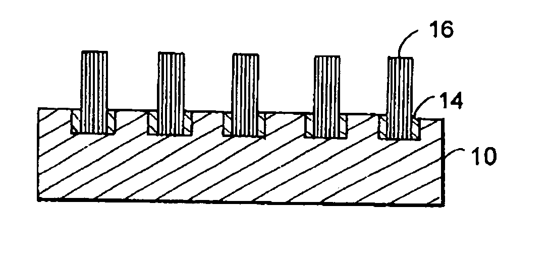
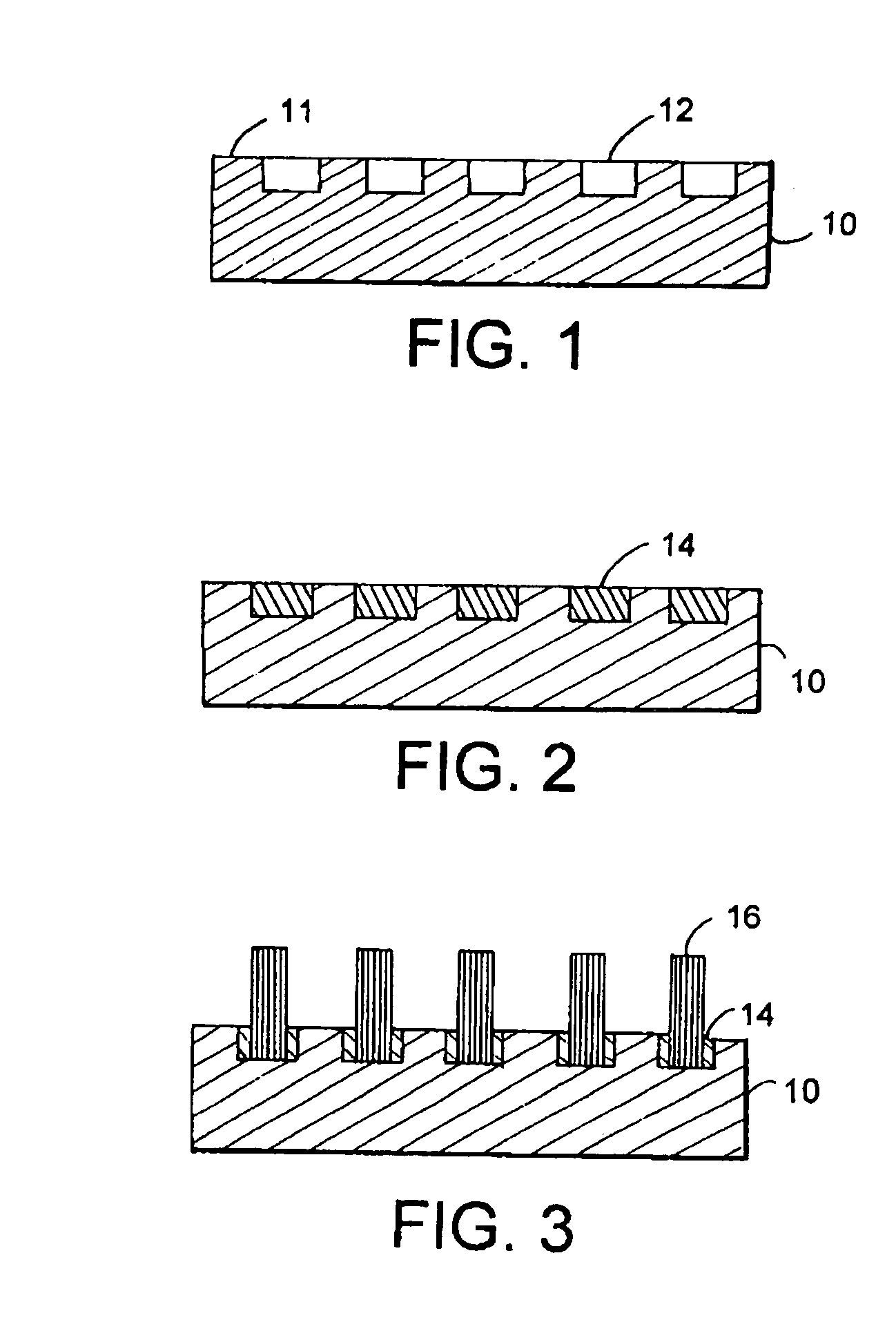
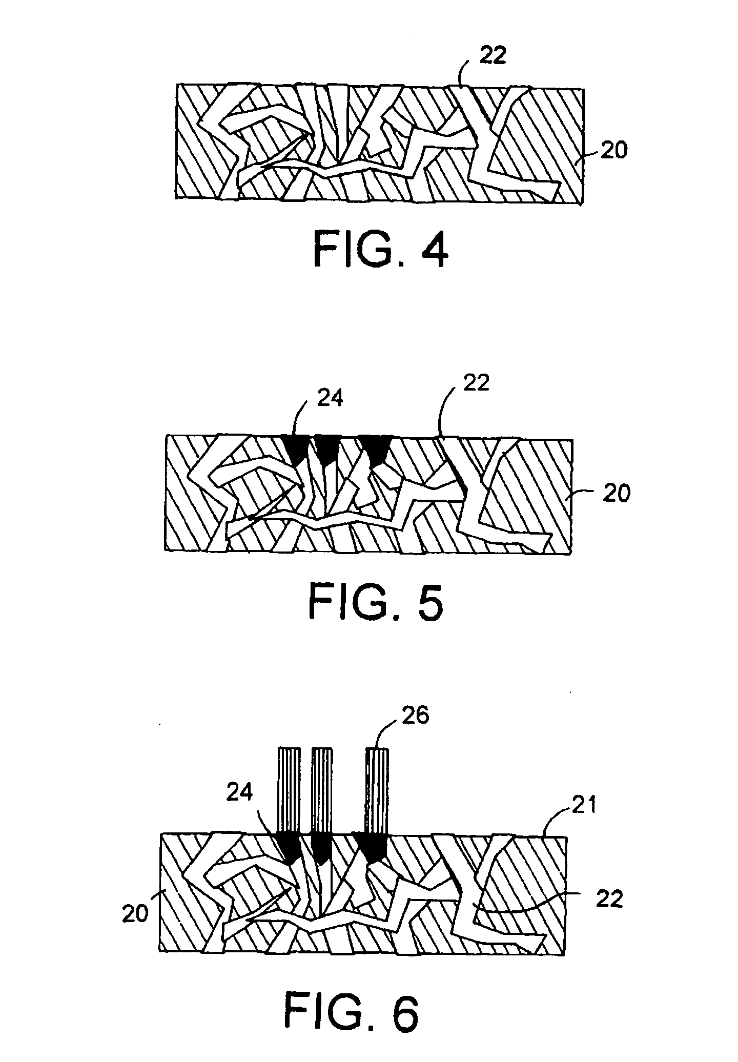
Image

Examples
example i
Comparative Example—Nanotube Growth on CoMo Bulk Powder on Solid Glass
[0039] Cobalt(II) molybdenum oxide, CoMoO4, 99.9% (metal basis), from Alfa Aesar, was used to test the activity of CoMo catalyst alone for carbon nanotube growth. A thin layer of the solid powder was gently distributed on a high purity fused silica glass (Corning's HPFS® fused silica glass marketed under glass code 7980) surface. The HPFS glass is a dense material and has a high melting point. The glass slide was placed in a flow reactor apparatus made of quartz tube of about 19 mm inner diameter. The quartz tube reactor was heated by a three-zone Lindberg furnace. The growth conditions and procedure consisted of (1) calcining the catalyst sample in flowing air by raising the temperature to 250° C. at 2° C. / min. in flowing air and holding overnight at 250° C. in the flowing air, (2) purging the reactor tube with inert nitrogen gas for about 10 min., (3) reducing the catalyst in flowing 10% H2 / Ar gas by raising t...
example ii
Comparative Example—Nanotube Growth on CoMo+Silica Sol on Solid Glass
[0042] 4 grams of the CoMoO4 powder as used in Example I were added into 20 gram of silica colloidal solution, 4 nm of silica particle size, 15 wt. % silica in water, from Alfa Aesar. The mixture was vigorously stirred about 30 min. The mixed solution turned a greenish color. The mixture was left overnight for sedimentation of the larger particles. The solution was spread onto the solid HPFS glass surface as used in Example I. The glass slide was placed inside a quartz tube reactor and reacted with the 25% CO / Ar gas at 650° C. for 32 h. The procedure and other conditions were the same as in Example I.
[0043] The top layer made of black powder-like material was peeled off from the HPFS glass substrate. No attachment to the glass surface was visibly seen. The black powder was analyzed with SEM. As illustrated in FIG. 8, massive carbonaceous deposition was found. Those materials looked like graphitic fibers and amorp...
example iii
Comparative Example—CoMo-Silica Sol on Solid Glass
[0044] Sol gel method is used in this example for deposition of catalytic materials on a dense, solid glass surface. The glass substrate (Corning's LCD glass marketed under glass code 1737) was about 0.9 mm thick, dense, and had a smooth surface designed for liquid-crystal display (LCD) application. 7.7 cc of an aqueous solution with concentration of 0.5M Co and 0.5M Mo, was mixed with 35 cc of tetraethoxysilane (TEOS) solution (Aldrich). The two phases were not miscible. 1.4 cc of 30 wt. % HCl solution were gradually added into the mixture. The solution was mixed for about 30 min. under stirring. A clear sol of blue was formed. The sol solution was used to dipcoat a glass slide designed for the LCD application. The glass surface was smooth and dense. The glass slide was placed inside a quartz tube reactor and reacted with the 25% CO / Ar gas at 700° C. for 2 h. The procedure and other conditions were similar to those in Example I.
[0...
PUM
| Property | Measurement | Unit |
|---|---|---|
| softening point temperature | aaaaa | aaaaa |
| size | aaaaa | aaaaa |
| size | aaaaa | aaaaa |
Abstract
Description
Claims
Application Information
 - R&D
- Intellectual Property
- Life Sciences
- Materials
- Tech Scout
- Unparalleled Data Quality
- Higher Quality Content
- 60% Fewer Hallucinations
Browse by: Latest US Patents, China's latest patents, Technical Efficacy Thesaurus, Application Domain, Technology Topic, Popular Technical Reports.
© 2025 PatSnap. All rights reserved.Legal|Privacy policy|Modern Slavery Act Transparency Statement|Sitemap|About US| Contact US: help@patsnap.com