

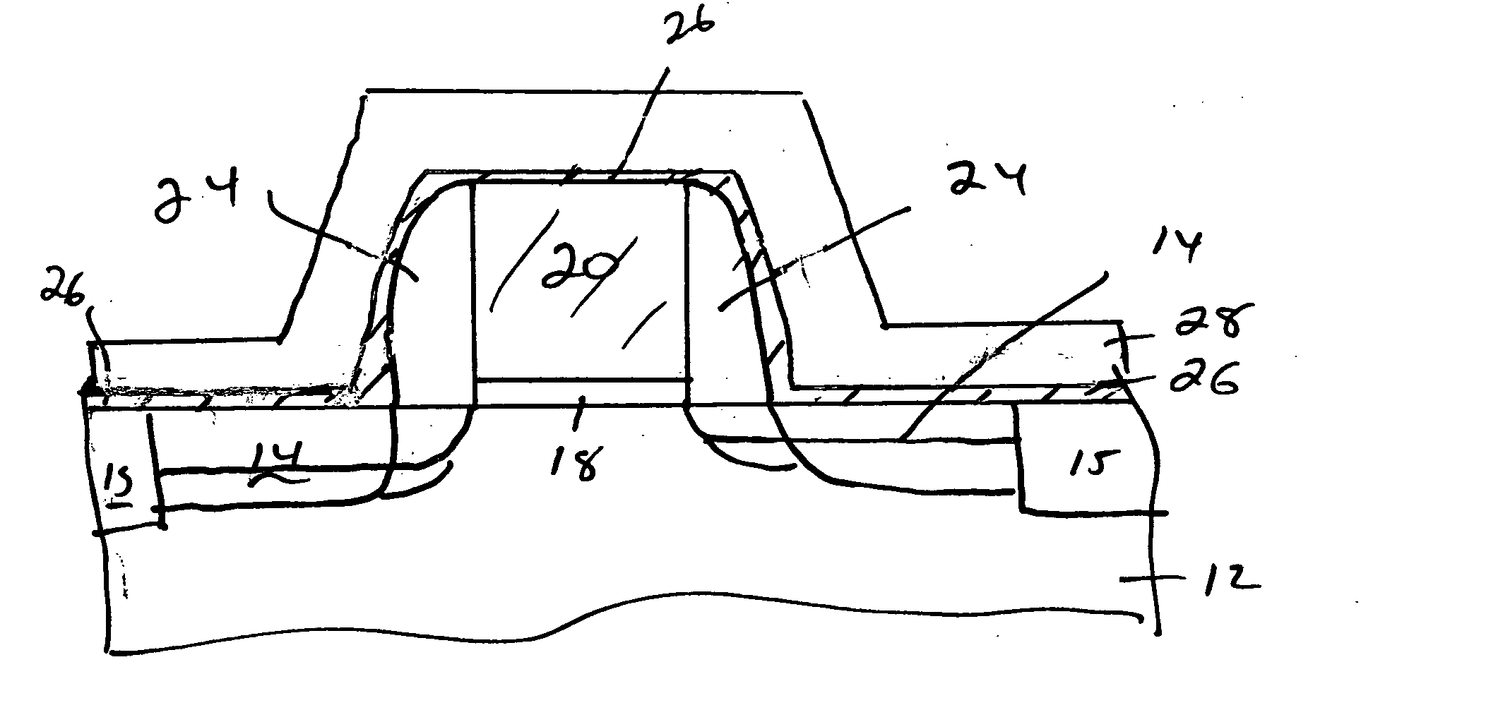
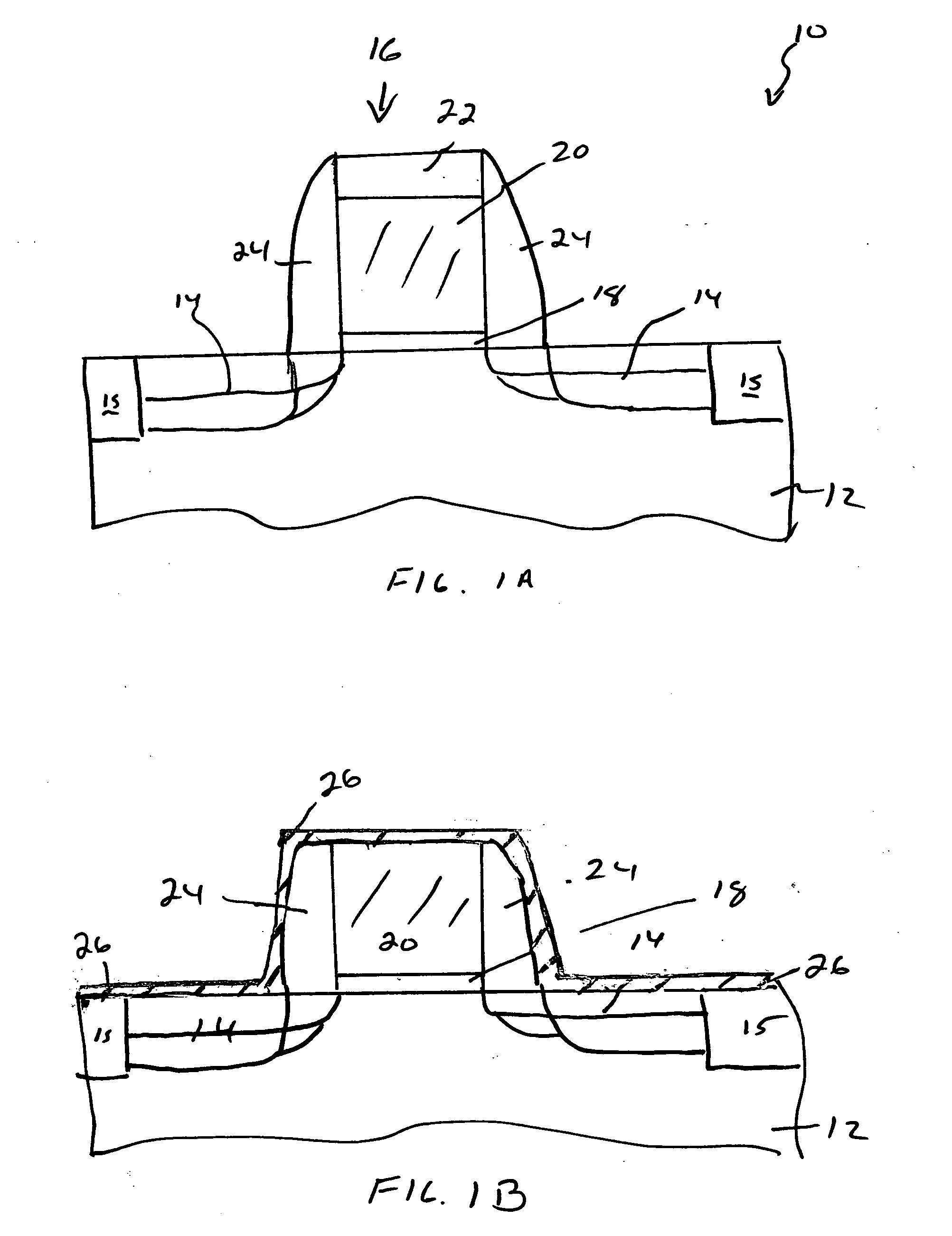
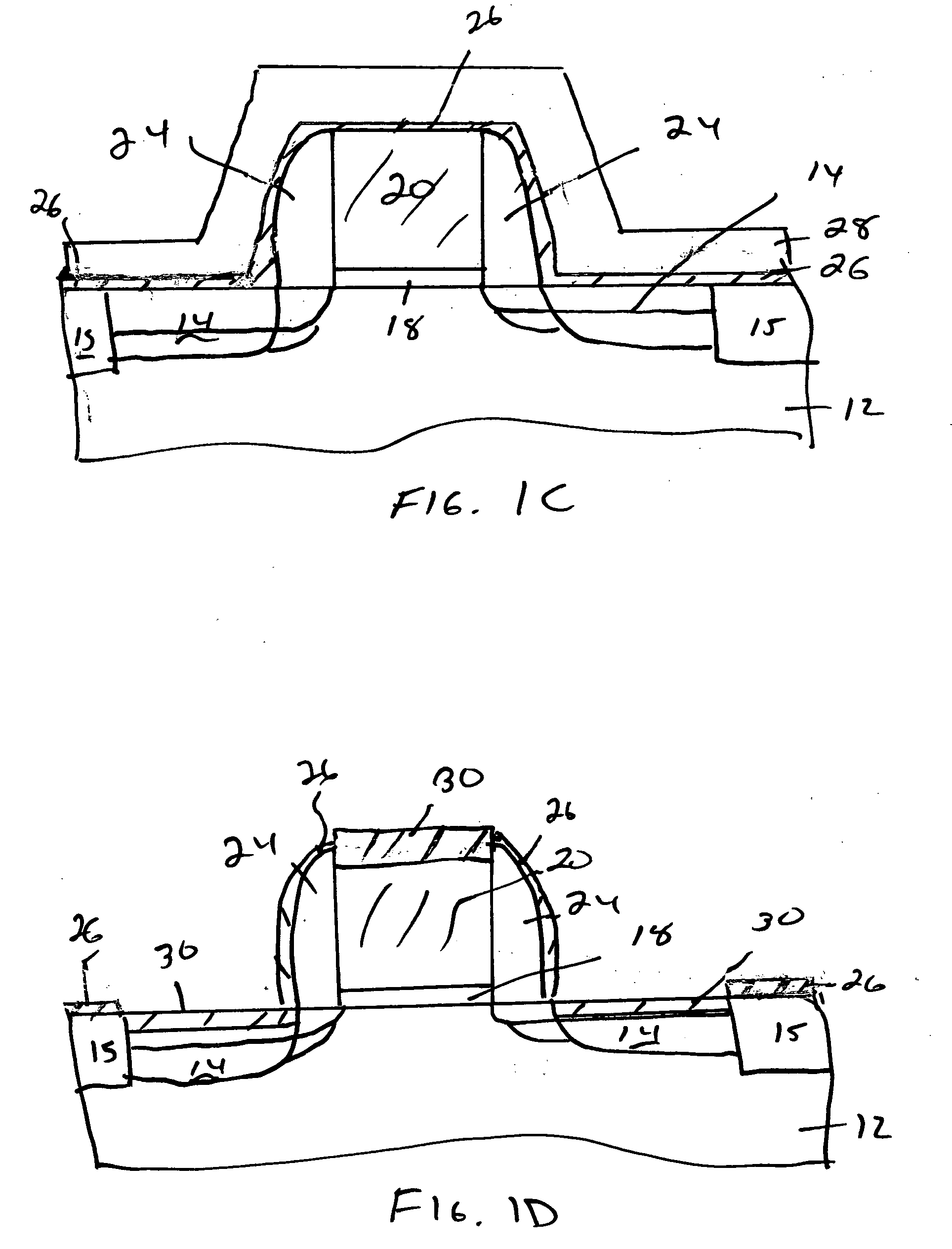
Method and process for forming a self-aligned silicide contact
a metal silicide and contact technology, applied in the direction of semiconductor devices, basic electric elements, electrical equipment, etc., can solve the problems of increasing the difficulty of forming shallow junctions for silicon-on-insulator (soi) substrates, sub>2 /sub>also exhibits rapid sheet resistance degradation, and shortening the device between the gate and the source/drain region
- Summary
- Abstract
- Description
- Claims
- Application Information
AI Technical Summary
Benefits of technology
Problems solved by technology
Method used
Image

Examples
example 1
[0072] This example illustrates the problem with using the prior art etching solution (mixture of hydrogen peroxide and sulfuric acid) which leaves stringers of Pt on the spacers and the trench isolation regions. Reference is made first to FIG. 3 which is a top-down SEM image of SRAM cell with Ni—Pt silicide contact which was prepared using the processing steps described above except that the etching solution was a conventional solution of hydrogen peroxide and sulfuric acid. Incomplete removal of metals was seen with this etch (Hydrogen peroxide, sulfuric acid mixture). AES analysis of stringers (unreacted metal) reveals that they were platinum.
[0073]FIG. 4 is a cross-section image of an NFET with Ni—Pt silicide contact prepared using the above processing steps except that the conventional etch solution described above was employed. Presence of unreacted metal on the spacer was seen after this etch which could lead to shorting of the device between the gate and the source / drain re...
example 2
[0074] This example illustrates the importance of utilizing the processing steps of the present invention. Specifically, FIG. 5 illustrates the change in sheet resistance of NiPt Alloy samples with different anneal temperatures. In this instance, samples were annealed in an inert (nitrogen) atmosphere with less than 1 ppm oxygen to prevent oxidation of metals. The temperature of the blanket layer was raised from ambient temperature to 150°-500° C. at a ramp rate of 5° C. / s. Each sample was held at the desired temperature for 5 seconds and subsequently brought back to room temperature. The sheet resistance for both NiPt and NiPtRe wafers remained high at temperatures less than 350° C. and decreases dramatically beyond 350° C. The high Rs corresponds with metal rich phases such as Ni2Si, Ni3Si, Ni31Si12. The change in Rs can be directly correlated to the formation of the monosilicide phase. The transition from metal rich phases to NiSi is sharper in NiPtRe as compared to NiPt. Further...
PUM
| Property | Measurement | Unit |
|---|---|---|
| temperature | aaaaa | aaaaa |
| temperature | aaaaa | aaaaa |
| time period | aaaaa | aaaaa |
Abstract
Description
Claims
Application Information