Biased pulse DC reactive sputtering of oxide films

a technology of reactive sputtering and oxide films, applied in the direction of instruments, optical elements, vacuum evaporation coatings, etc., can solve the problems of difficult control of uniformity of doping in cvd processes, phosphorous and boron are hygroscopic, and alkalis are undesirable for integration with electronic devices

Inactive Publication Date: 2006-03-16
DEMARAY
View PDF99 Cites 54 Cited by
  • Summary
  • Abstract
  • Description
  • Claims
  • Application Information

AI Technical Summary

Problems solved by technology

However, dopants such as phosphorous and boron are hygroscopic, and alkalis are undesirable for integration with electronic devices.
Control of uniformity of doping in CVD processes can be difficult and CVD deposited films can have structural defects leading to scattering losses when used to guide light.
In addition, doped low temperature glasses may require further processing after deposition.
Since the tiles can not be made very large, there may be a large problem of arcing between tiles and therefore contamination of the deposited film due to this arcing.
Further, the reactors required for RF sputtering tend to be rather complicated.
In particular, the engineering of low capacitance efficient RF power distribution to the cathode is difficult in RF systems.

Method used


Image

  • Biased pulse DC reactive sputtering of oxide films
  • Biased pulse DC reactive sputtering of oxide films
  • Biased pulse DC reactive sputtering of oxide films

Examples


example 1

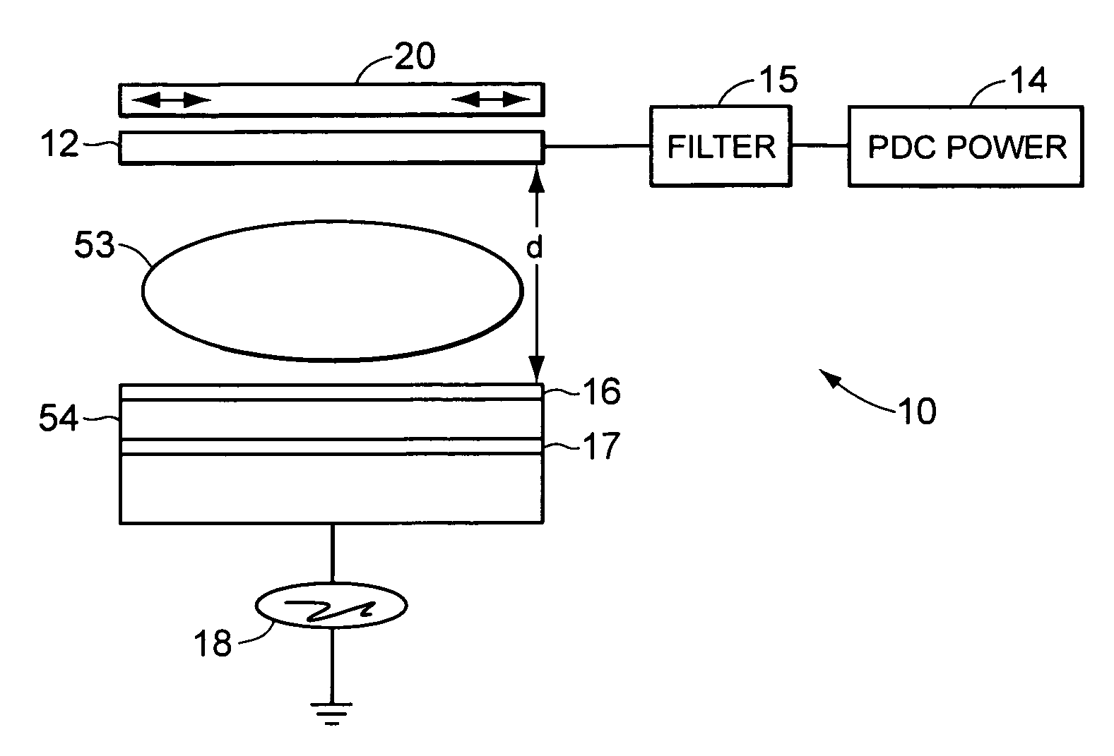
[0114] An AKT 1600 based reactor can be utilized to deposit a film. In this example, a wide area metallic target of dimension 550×650 mm with composition (Si / Al / Er / Yb) being about 57.0 cat. % Si, 41.4 cat. % Al, 0.8 cat. % Er, and 0.8 cat. % Yb (a “0.8 / 0.8” target) was fabricated as described in the '247 patent.

[0115] In step 402, a 150 mm P-type silicon wafer substrate was placed in the center of a 400×500 mm glass carrier sheet 17. Power supply 14 was set to supply 6000 watts of pulse DC power at a frequency of 120 KHz with a reverse pulsing time of about 2.3 us. Magnet 20, which is a race-track shaped magnet of approximate dimension 150 mm×600 mm, was swept over the backside of the target at a rate of about 4 seconds per one-way scan. The temperature of substrate 16 was held at 200 C and 100W of 2 MHz RF power was applied to substrate 16. The target 12 to substrate 16 distance was about 6.5 cm. The sputtering gas was a mixture of Argon and Oxygen. Substrate 16 and carrier 17 was...

example 2

[0121] A waveguide amplifier can be deposited according to the present invention. An embodiment of target 12 having composition 57.4 cat. % Si, 41.0 cat. % Al, 0.8 cat. % Er 0.8 cat. % Yb (the “0.8 / 0.8 target”) can be formed as disclosed in the '245 application. The Er—Yb (0.8 / 0.8) co-doped Alumino-Silicate film was deposited onto a 6 inch wafer of substrate 16 which includes a 10 μm thick thermal oxide substrate, which can be purchased from companies such as Silicon Quest International, Santa Clara, Calif. Target 12 was first cleaned by sputtering with Ar (80 sccm) only in the metallic mode. Target 12 was then conditioned in poison mode by flowing 60 sccm of Argon and 40 sccm of oxygen respectively. The power supplied to target 12 during conditioning was kept at about 6 kW.

[0122] An active core film was then deposited on substrate 16. The thickness of the deposited film is approximately 1.2 μm. The deposition parameters are shown in Table 2.

TABLE 2TargetPulsingReversePowerAr / O2F...

example 3

[0125] This example describes production of a dual core Erbiurn / Yttrbium co-doped amplifier according to the present invention. In one example, substrate 16 is a silicon substrate with an undercladding layer of thermally oxidized SiO2 of about 15 μm thick. Substrate 16 with the thermal oxide layer can be purchased from companies such as Silicon Quest International, Santa Clara, Calif. A layer of active core material is then deposited on substrate 16 with a Shadow Mask as described in the '138 application. Use of a shadow mask results in a vertical taper on each side of a finished waveguide which greatly enhances the coupling of light into and out of the waveguide.

[0126] Active core layer is deposited from a 0.8 / 0.8 target as described in the '247 application having composition 57.4 cat. % Si, 41.0 cat. % Al, 0.8 cat. % Er, and 0.8 cat. % Yb. The deposition parameters are identical to that of Example 2 described above. The active layer is deposited to a thickness of about 1.2 μm.

[0...


PUM


Abstract

A biased pulse DC reactor for sputtering of oxide films is presented. The biased pulse DC reactor couples pulsed DC at a particular frequency to the target through a filter which filters out the effects of a bias power applied to the substrate, protecting the pulsed DC power supply. Films deposited utilizing the reactor have controllable material properties such as the index of refraction. Optical components such as waveguide amplifiers and multiplexers can be fabricated using processes performed on a reactor according to the present inention.

Description

BACKGROUND [0001] 1. Field of the Invention [0002] The present invention relates to deposition of oxide and oxynitride films and, in particular, to deposition of oxide and oxynitride films by pulsed DC reactive sputtering. [0003] 2. Discussion of Related Art [0004] Deposition of insulating materials and especially optical materials is technologically important in several areas including production of optical devices and production of semiconductor devices. In semiconductor devices, doped alumina silicates can be utilized as high dielectric insulators. [0005] The increasing prevalence of fiber optic communications systems has created an unprecedented demand for devices for processing optical signals. Planar devices such as optical waveguides, couplers, splitters, and amplifiers, fabricated on planar substrates, like those commonly used for integrated circuits, and configured to receive and process signals from optical fibers are highly desirable. Such devices hold promise for integra...

Claims


Application Information

Patent Timeline
Patent Type & Authority Applications(United States)
IPC IPC(8): B05D5/06C23C14/00C23C14/34C23C14/35G02B6/132H01J37/34
CPCC23C14/0036C23C14/081C23C14/10C23C14/3414C23C14/345H01J37/34C23C14/354C23C14/5806C23C14/5873G02B6/132H01J37/32412C23C14/35
Inventor ZHANG, HONGMEINARASIMHAN, MUKUNDANMULLAPUDI, RAVI B.DEMARAY, RICHARD E.
Owner DEMARAY
Why Eureka
Try Eureka