Novel polyorganosiloxane dielectric materials

a dielectric material and polyorganosiloxane technology, applied in the field of thin films, can solve the problems of reducing the degree of bridging crosslinking between organic units and films, limited application of these films, and low thermal stability, and achieves excellent chemical resistance, low chemical adsorption behavior, and high cross-linking

Active Publication Date: 2006-03-16
SILECS OY
View PDF15 Cites 16 Cited by
  • Summary
  • Abstract
  • Description
  • Claims
  • Application Information

AI Technical Summary

Benefits of technology

[0041] Considerable advantages are obtained by the present novel materials and by the methods of manufacturing them. Thus, the present invention presents a solution for existing problems related to low-k dielectric polymers, more specifically mechanical properties (modulus and hardness), cracking threshold and thermal properties, especially applicable for aluminum reflow processing temperatures (also known as hot aluminum process). At the same time, the present invention provides excellent chemical resistance and very low chemical adsorption behavior due to high cross-linking bridging group density.
[0042] Another important advantages is that the novel low-k dielectric materials have excellent properties of planarization resulting in excellent local and global planarity on top a semiconductor substrate topography, which reduces or even fully eliminates the need for chemical mechanical planarization after dielectric and oxide liner deposition.
[0043] Furthermore, the novel materials have excellent gap fill properties.

Problems solved by technology

However, applicability of these films is limited because of their low thermal stability, softness, and incompatibility with traditional technological processes developed for SiO2 based dielectrics.
However, these organic units reduce the degrees of bridging crosslinks as well increases the free volume between the molecules due to steric hindrance.

Method used


Image

  • Novel polyorganosiloxane dielectric materials
  • Novel polyorganosiloxane dielectric materials
  • Novel polyorganosiloxane dielectric materials

Examples


example 1

[0105] Vinyltrichlorosilane, in an amount of 142.2 g (0.880 mol), and 5 ml (5.55 g, 0.048 mol) methyldichlorosilane were introduced into a 500 ml vessel. The solution was heated up to 80° C. and 15 μl H2PtCl6 / IPA catalyst solution was added. Exothermic reaction was observed immediately and heat was switched off. Rest of the methyldichlorosilane was added in ˜20 ml portions during 30 min so that temperature of the solution did not raise over 130° C. The total amount of methyldichlorosilane was 104.2 g (0.906 mol, 2.9% excess). The solution was again heated up to 110° C. and stirred for an hour. The obtained solution was distilled. B.p. was 77° C. / 10 mbar and yield was 188 g (77%). The product, 1-(trichlorosilyl)-2-(methyldichlorosilyl) ethane, was analyzed with GC, 13C and 29Si NMR.

[0106] The synthesized molecule, 1-(trichlorosilyl)-2-(methyldichlorosilyl) ethane, (25.00 g, 0.090 mol) was weighed and dissolved to 100 ml methyl t-butyl ether (MTBE). The solution was transferred drop ...

example 2

[0114] The present invention also encompasses isomers of 1-(trichlorosilyl)-2-(methyldichlorosilyl) ethane. Methyldichlorosilane (14.9 g, 0.130 mol), vinyl trichlorosilane (21.0 g, 0.130 mol) and 100 mg tetrakis(triphenylphosphine)palladium were placed in a glass pressure tube and heated to 105° C. After ˜20 minutes, vigorous exothermic reaction too place and the solution turned dark. The content was distilled at 74° C. / 5 mbar to give 32.3 g (0.117 mol, 90%). Purity was >99% by GC. The resulting monomer was 1-(methyldichlorosilyl)-1-(trichlorosilyl) ethane.

example 3

Alternative Method for Polymer

[0115] Examples 1 and 2 describe the synthesis of two monomers, i.e., 1-(trichlorosilyl)-2-(methyldichlorosilyl) ethane and 1-(methyldichlorosilyl)-1-(trichlorosilyl) ethane, which can be used as precursors of polymers.

1(Trichlorosilyl)-2- (methyldichlorosilyl) ethane

1-(Methyldichlorosilyl)-1-(trichlorosilyl) ethane

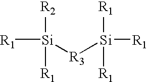
[0116] These isomer compounds, one of which is comprising a linear linker chain and the other a branched linker chain, can be used in any ratio to form the novel dielectric siloxane polymers according to the present invention. Thus, the monomer comprising the linear linker molecule can be employed at a molar ratios of 1:100 to 100:1, preferably 80:20 to 20:80, in particular 60:40 to 40:60, with respect to the corresponding monomer comprising the branched linker molecule.


PUM


Abstract

A thin film comprising a composition obtained by polymerizing a monomer having the formula I:
wherein:
    • R1 is a hydrolysable group,
    • R2 is a polarizability reducing organic group, and
    • R3 is a bridging hydrocarbon group, to form a siloxane material. The invention also concerns methods for producing the thin films. The thin film can be used a low k dielectric in integrated circuit devices. The novel dielectric materials have excellent properties of planarization resulting in good local and global planarity on top a semiconductor substrate topography, which reduces or eliminates the need for chemical mechanical planarization after dielectric and oxide liner deposition.

Description

[0001] This application claims priority of U.S. Provisional Applications for Patent Serial No. 60 / 605,553 filed Aug. 31, 2004, and 60 / 644,304 filed Jan. 18, 2005, which are incorporated herein by reference.BACKGROUND OF THE INVENTION [0002] 1. Field of the Invention [0003] The present invention relates to thin films suitable as dielectrics in IC's and for other similar applications. In particular, the invention concerns thin films comprising compositions obtainable by polymerization of silicon containing monomers, which yield an at least partially cross-linked siloxane structure. The invention also concerns a method for producing such films by preparing siloxane compositions by polymerization of the monomers, by applying the polymerized compositions on a substrate in the form of a layer and by curing the layer to form a film. Further, the invention concerns integrated circuit devices and methods of manufacturing them. [0004] 2. Description of Related Art [0005] Built on semiconducto...

Claims


Application Information

Patent Timeline
Patent Type & Authority Applications(United States)
IPC IPC(8): C08G77/04C08L83/04B05D3/02B32B9/04
CPCC08G77/50C09D183/14H01B3/46H01L21/02126H01L21/02282H01L21/3122H01L21/76822H01L2924/0002H01L21/76837H01L23/5329H01L2924/12044H01L2924/00Y10T428/31663
Inventor RANTALA, JUHA T.PAULASAARI, JYRIKYLMA, JANNETORMANEN, TURO T.PIETIKAINEN, JARKKOHACKER, NIGELHADZIC, ADMIR
Owner SILECS OY
Why Eureka
Try Eureka