

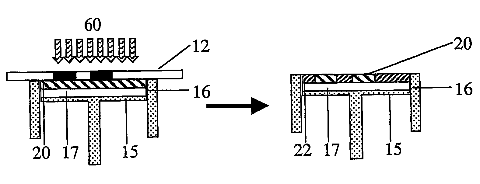
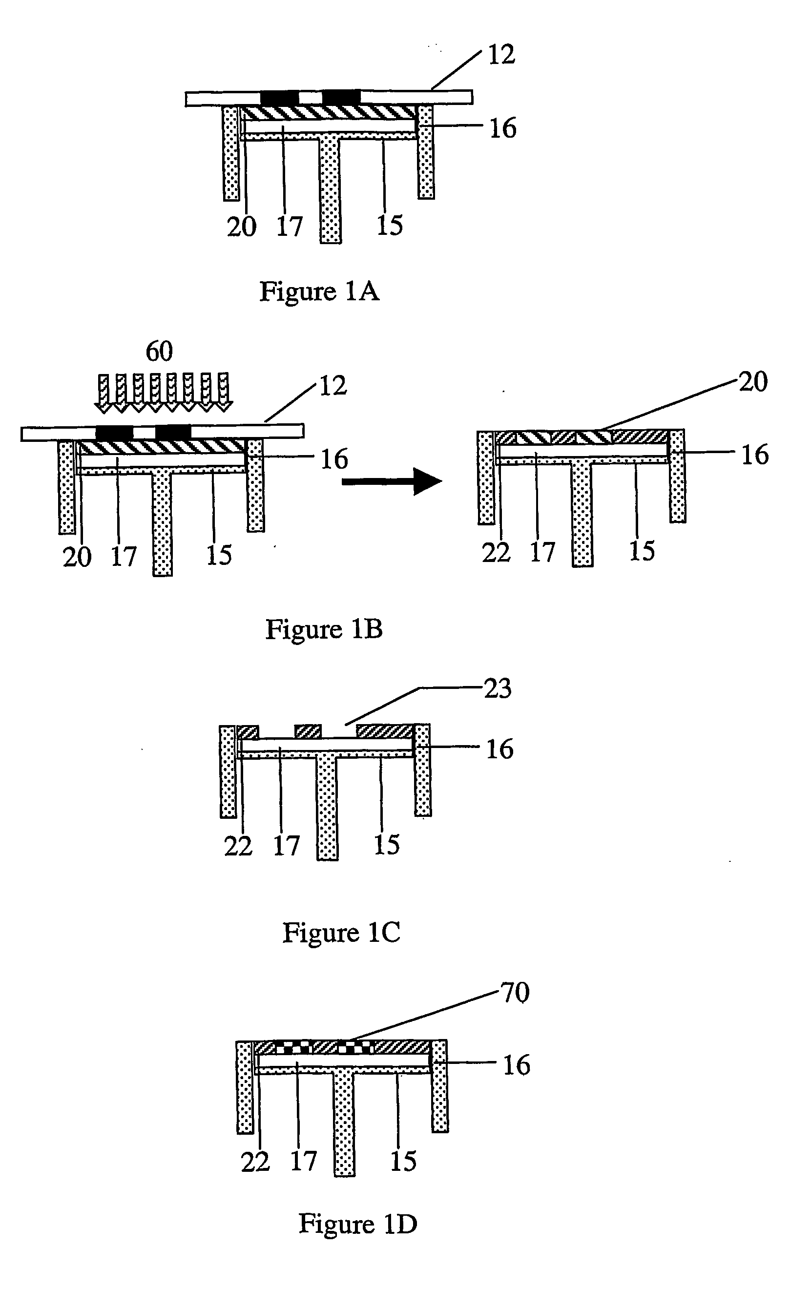
Fabrication of 3d photopolymeric devices
a technology of polymer devices and fabrication methods, applied in the direction of photomechanical devices, manufacturing tools, instruments, etc., can solve the problems of limited design to one layer, long time required for high-resolution microstructure fabrication, and inability to facilitate high-parallele fabrication
- Summary
- Abstract
- Description
- Claims
- Application Information
AI Technical Summary
Benefits of technology
Problems solved by technology
Method used
Image

Examples
example 1
Apparatus for Fabrication of Photopolymeric Devices
[0100] The apparatus for photopolymeric device fabrication was based on a photolithography system from Optical Associates, Inc., San Jose, Calif. The original mask alignment system (Model 204) was equipped with micropositioners in the x, y, z, and theta directions. The opening in the mask holder of the original system was enlarged and the substrate holder (i.e., wafer chuck housing) replaced with a reaction chamber. An LVDT height measurement sensor also added (220 in FIG. 6B). The collimated flood exposure source used with the system provided 50 to 70 mW / cm2 of 365-nm radiation.
[0101]FIGS. 6A-6D show an exemplary apparatus for fabrication of photopolymeric devices. FIG. 6A shows the photomask holder (200) which was supported at the back by a hinge (210) and at the front by two posts (215). The printed photomask (not shown) was attached to a glass plate (not shown) which was attached to the photomask holder with clamps. FIG. 6B il...
example 2
Fabrication of Photopolymeric Devices
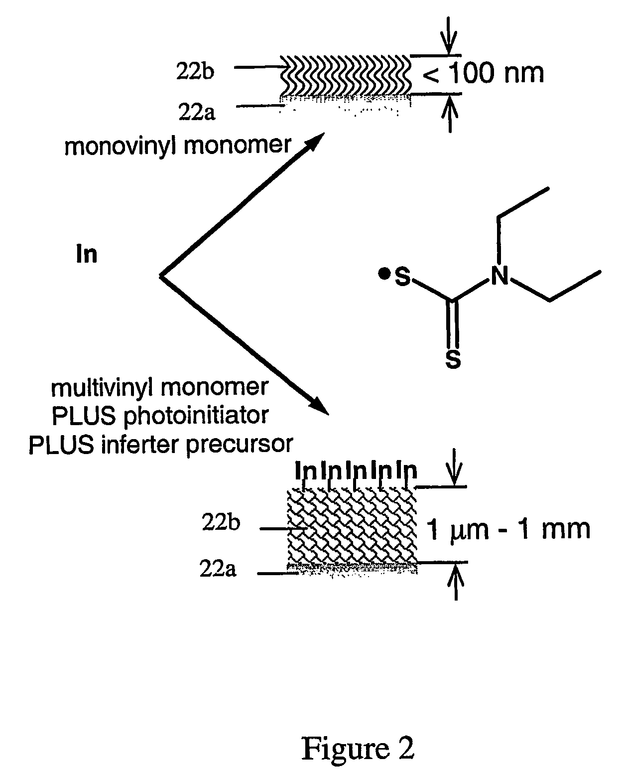
[0103] A typical monomer formulation for structures included 1.5% (wt / wt) 1-hydroxycyclohexyl phenyl ketone (tradename: Irgacure 184, Ciba, Tarrytown, N.Y.) as the photoinitiator, 1.0% photoiniferter precursor, tetraethylthiuram disulfide (TED, Aldrich Chemical Co., Milwaukee, Wis.), and 1.0% acrylic acid (Aldrich), in a mixture of 50% (wt / wt) triethyleneglycol diacrylate (Sartomer, Exton, Pa.) and 50% hexavinyl aromatic urethane acrylate (EBECRYL 220, Sartomer). For multilayer structures, paraffin wax was used as a sacrificial material.
[0104] Typically, a polycarbonate substrate was attached to a metal bottom plate with a two-part epoxy. The metal plate was fixed to the adjustable bottom of the chamber with two or more machine screws. The photomask was printed on a transparency film and attached to a glass plate with a photosensitive adhesive. The glass plate was secured with the original mask clamps. The distance between the polycarbonate sub...
PUM
| Property | Measurement | Unit |
|---|---|---|
| diameter | aaaaa | aaaaa |
| thickness | aaaaa | aaaaa |
| thickness | aaaaa | aaaaa |
Abstract
Description
Claims
Application Information