Method of modifying an etched trench

a technology of etching and etching, which is applied in the direction of recording equipment, instruments, and recording information storage, etc., can solve the problems of slowing down the etching rate, placing considerable demands on the etching method employed, and etching the ink supply channel, so as to reduce reduce the degree of flaring. , the effect of reducing the angle of flaring

Inactive Publication Date: 2006-04-13
MEMJET TECH LTD
View PDF5 Cites 7 Cited by
  • Summary
  • Abstract
  • Description
  • Claims
  • Application Information

AI Technical Summary

Benefits of technology

[0046] By using a source of O2 plasma, which is biased in a plasma etching chamber, the O2 plasma has sufficient energy to remove polymeric residues in deep (e.g. over 100 micron deep) trenches at a temperature lower than the release temperature of standard thermal release tape.
[0047] With reference to the third, fourth and fifth aspects of the present application, hitherto, the importance of the surface profile of ink supply channels in printheads fabricated by MEMS techniques had not been fully appreciated. Whilst several ultradeep etching techniques have become available in recent years, none of these addresses the problems described above when back-etching towards (and beyond) a photoresist plug. In particular, the problem of a sharp, potentially frangible, circumferential rim being formed in the sidewalls had not been addressed. As discussed above, this rim is formed during back-etching as the etch front radially flares around the photoresist plug (see FIGS. 4 and 5).
[0048] The problem of an etch front radially flaring around a photoresist plug can be addressed, to some extent, by special etching techniques. An example of one such special etching technique is described in U.S. Pat. No. 6,187,685 (assigned to Surface Technology Systems). However, whilst the technique described in U.S. Pat. No. 6,187,685 can reduce the angle of flaring relative to the perpendicular, it still does not completely eliminate the formation of a circumferential rim around the photoresist plug. Indeed, since the resultant rim is made

Problems solved by technology

These ink channels are typically etched through wafers having a thickness of about 200 □m, and therefore place considerable demands on the etching method employed.
However, there are a number of problems associated with back-etching the ink supply channels in this way.
However, a major disadvantage of the Bosch process is that polymer deposition and etching steps need to be alternated, which means continuously alternating the gas composition of the plasma, thereby slowing etch rates.
A further disadvantage of the Bosch process is that it leaves a hydrophobic fluorocarbon polymer coating (‘Bosch polymer’) on the trench sidewalls.
However, both O2 ashing and EKC™ cleans suffer from serious problems during MEMS processing of a silicon wafer.
Lowering the temperature of ashing oven produces unacceptably low

Method used


Image

  • Method of modifying an etched trench
  • Method of modifying an etched trench
  • Method of modifying an etched trench

Examples


example

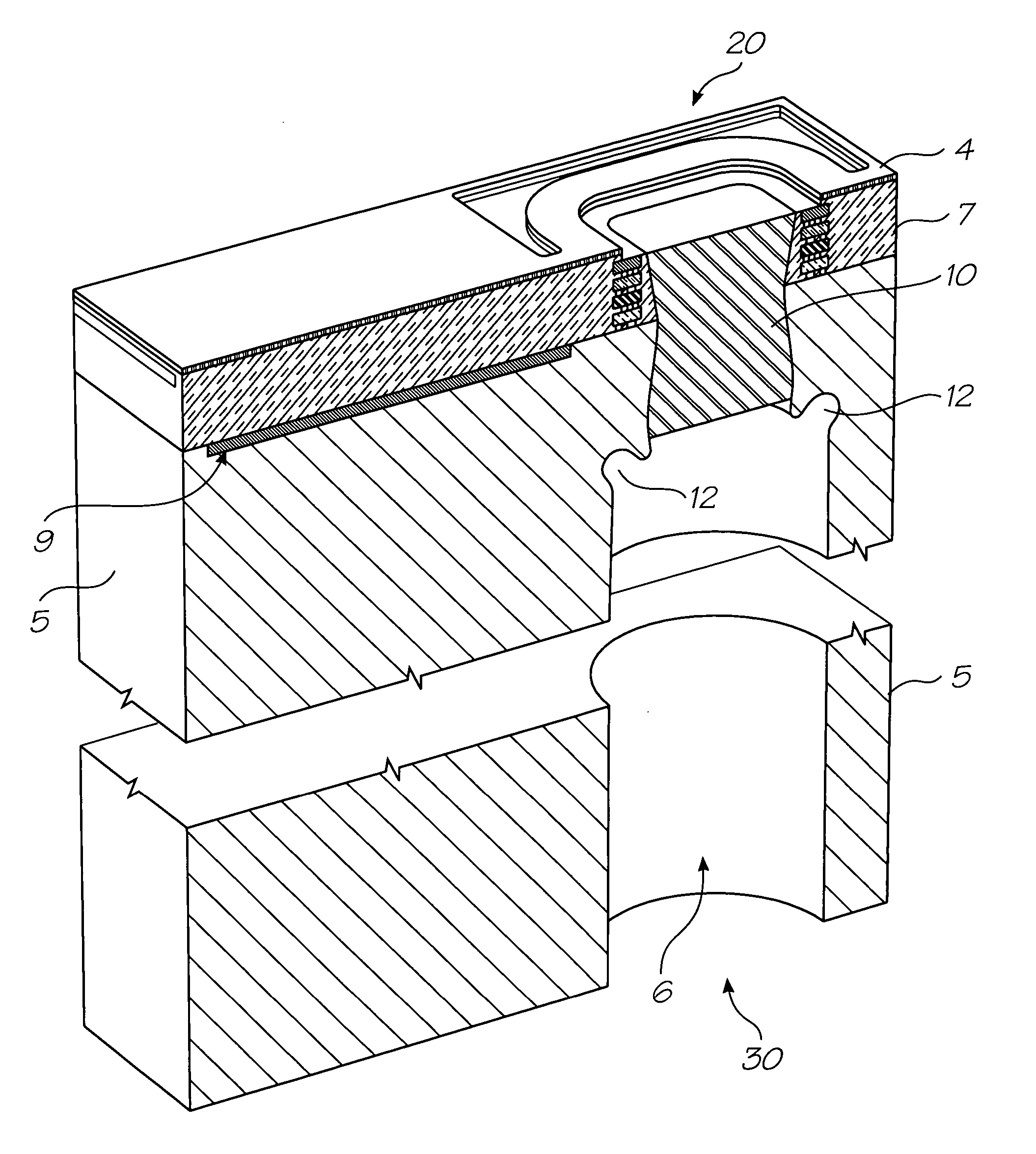
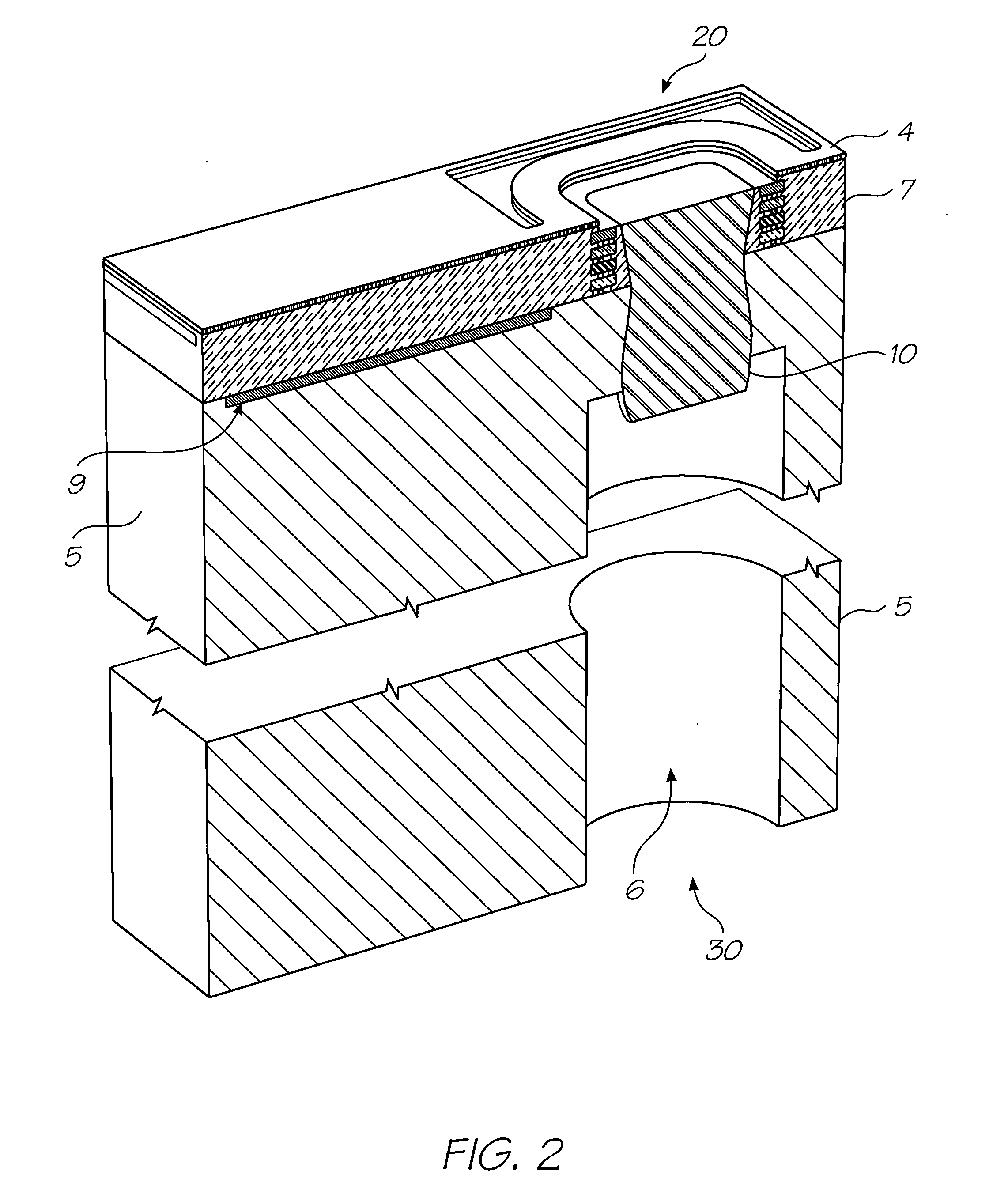
[0143] A silicon wafer having a thickness of 200 □m was prepared as follows. Using a standard anisotropic DRIE process a trench, having a diameter of 14 □m and a depth of 28 □m, was etched into a frontside of the wafer. The trench was filled with photoresist to form a front plug. With the frontside of the wafer attached to a glass handle wafer, the backside is then etched to within 5 □m of the back surface of the front plug. Again, a standard anisotropic DRIE process is used for backside etching. The back-etched main trench had a depth of about 170 □m and a diameter of about 21 □m. FIG. 9 is an SEM micrograph of the silicon wafer after back-etching to within 5 □m of the front plug.

[0144] Back-etching was continued to the back surface of the front plug and about 5 □m past the front plug, under anisotropic etching conditions. FIG. 10 is an SEM micrograph of part of the trench after back-etching past the front plug. As shown in FIG. 10, a spiked circumferential rim extends around the ...


PUM

PropertyMeasurementUnit
Pressureaaaaaaaaaa
Poweraaaaaaaaaa
Poweraaaaaaaaaa

Abstract

A process for facilitating modification of an etched trench is provided. The process comprises: (a) providing a wafer comprising an etched trench, the trench having a photoresist plug at its base; and (b) removing a portion of the photoresist by subjecting the wafer to a biased oxygen plasma etch. The process is particularly suitable for preparing a trench for subsequent argon ion milling. Printhead integrated circuits fabricated by a process according to the invention have improved ink channel surface profiles and/or surface properties.

Description

FIELD OF THE INVENTION [0001] This invention relates to a process for modifying sidewalls of a trench etched into a semiconductor wafer. It has been developed primarily for incorporation into a printhead integrated circuit manufacturing process in order to provide an ink channel having improved surface properties and / or improved surface profile. However, it may equally be incorporated into any etching process. COPENDING APPLICATIONS [0002] The following application has been filed by the applicant simultaneously with the present application: [0003] MEMS27US The disclosure of this copending application is incorporated herein by reference. The above application has been identified by its filing docket number, which will be substituted with the corresponding application number once assigned. CROSS REFERENCES TO RELATED APPLICATIONS [0004] Various methods, systems and apparatus relating to the present invention are disclosed in the following US Patents / Patent Applications filed by the a...

Claims


Application Information

Patent Timeline
IPC IPC(8): C23F1/00G01D15/00
CPCB41J2/1412B41J2/1601B41J2/1623B41J2/1628B41J2/1631B41J2/164B81B2201/052B81B2203/033B81C1/00849B81C2201/0112B81C2201/0132H01L21/02057H01L21/3065H01L27/00
Inventor MCREYNOLDS, DARRELL LARUESILVERBROOK, KIA
Owner MEMJET TECH LTD
Why Eureka
Try Eureka