Method to improve transmittance of an encapsulating film

a technology of encapsulating film and transmittance, which is applied in the direction of solid-state diffusion coating, plasma technique, superimposed coating process, etc., can solve the problems of material degradation and dark spot problems, reduce the life of display devices, and reduce the el efficiency and drive voltage. , to achieve the effect of improving the light transmittance of the amorphous carbon layer, improving the film uniformity of the amorphous carbon layer, and improving the light transmittance of th

Active Publication Date: 2006-04-13
APPLIED MATERIALS INC
View PDF19 Cites 49 Cited by
  • Summary
  • Abstract
  • Description
  • Claims
  • Application Information

AI Technical Summary

Benefits of technology

[0012] Embodiments of the invention generally provide a method and apparatus for depositing an encapsulating film onto a substrate. In one embodiment, a method for forming a multilayer encapsulating film onto a substrate placed in a substrate processing system includes depositing a plurality of silicon-containing inorganic barrier layers onto the surface of the substrate by delivering a first silicon-containing compound into the substrate processing system. The method further comprises depositing one or more carbon-containing material layers in between and / or alternating with the one or more silicon-containing inorganic barrier layers at a substrate temperature of about 200° C. or lower by delivering a mixture of precursors comprising a carbon-containing compound, a second silicon-containing compound, and a nitrogen-containing compound into the substrate processing system.
[0013] In another embodiment, a method for forming an amorphous carbon layer in a multilayer encapsulating film over a substrate within a substrate processing system includes delivering a hydrocarbon-containing precursor for the amorphous carbon layer, delivering a hydrogen gas adapted to improve the film uniformity of the amorphous carbon layer into the substrate processing system, and delivering a silicon-containing precursor and a nitrogen-containing precursor adapted to improve the light transmittance of the amorphous carbon layer to about 80% or higher at all wavelengths of a visible light spectrum into the substrate processing system. The method further includes controlling the temperature of the substrate to a temperature of about 150° C. or lower, generating a plasma to deposit the amorphous carbon layer on the surface of the substrate, and depositing the amorphous carbon layer onto the substrate until a desired thickness of the amorphous carbon layer is obtained.
[0014] In yet another embodiment, a method for depositing an encapsulating layer, having one or more layers of silicon-containing inorganic barrier materials and carbon-containing materials, onto a substrate in a substrate processing system is provided. The method includes delivering a first mixture of precursors for a silicon-containing inorganic barrier layer, delivering a hydrogen gas into the substrate processing system, controlling the temperature of the substrate to a temperature of about 150° C. or lower, and generating a plasma to deposit the silicon-containing inorganic barrier layer on the surface of the substrate. The method further includes delivering a second mixture of precursors for a carbon-containing material layer, delivering a hydrogen gas into the substrate processing system, controlling the temperature of the substrate to a temperature of about 150° C. or lower, and generating a plasma to deposit the carbon-containing material layer onto the surface of the silicon-containing inorganic barrier layer. The second mixture of precursors comprises a hydrocarbon-containing precursor, a silicon-containing precursor, and a nitrogen-containing precursor. The encapsulating layer is deposited onto the substrate until a thickness of the encapsulating layer of about 15,000 angstroms or more is obtained.
[0015] In still another embodiment, a method for forming an amorphous carbon layer in a multilayer encapsulating film over a substrate within a substrate processing system includes delivering a hydrocarbon-containing precursor at a first flow rate for the amorphous carbon layer and delivering a hydrogen gas adapted to improve the film uniformity of the amorphous carbon layer into the substrate processing system. The method further includes delivering a silicon-containing precursor at a second flow rate and a nitrogen-containing precursor at a third flow rate into the substrate processing system, controlling the temperature of the substrate to a temperature of about 150° C. or lower, and generating a plasma inside the substrate processing system for a time period, wherein the ratio of the first flow rate and the second flow rate is 4:1 or larger in order to deposit the amorphous carbon layer on the surface of the substrate and dope the amorphous carbon layer with silicon.
[0016] In still another embodiment, an apparatus to deposit a low temperature material layer onto a substrate is also provided. The apparatus includes, a substrate support disposed in a process chamber to support a substrate, such as a large area substrate, a RF source coupled to the process chamber to provide a plasma inside the process chamber, a silicon-containing compound supply source coupled to the process chamber, one or more nitrogen-containing compound supply sources coupled to the process chamber, a hydrogen gas supply source coupled to the process chamber, a carbon-containing compound supply source coupled to the process chamber, and a controller coupled to the process chamber to control the temperature of the substrate to about 200° C. or lower during substrate processing and adapted to deposit an encapsulating layer having one or more carbon-containing material layers in between one or more silicon-containing inorganic barrier layers.

Problems solved by technology

The lifetime of display devices can be limited, characterized by a decrease in EL efficiency and an increase in drive voltage, due to the degradation of organic or polymer materials, the formation of non-emissive dark spots, and crystallization of the organic layers at high temperature of about 55° C. or higher, e.g., crystallization of the hole transport materials.
In addition, the main reason for the material degradation and dark spot problems is moisture and oxygen ingress.
In addition, exposure to air or oxygen may cause cathode oxidation and once organic material reacts with water or oxygen, the organic material is dead.
However, moisture can easily penetrate through the epoxy and damage the device.
However, it is very difficult to generate water-barrier inorganic encapsulation materials using a low temperature deposition process because the resulting film is less dense and has high defect pinhole structures.
In addition, oxygen and humidity being trapped during encapsulation and infiltrating into the OLED device to be in contact with the cathode and organic materials generally result in dark spot formation, which is a frequent OLED destroying defect.
Other problems also arise when thin film inorganic silicon nitride (SiN) related materials are used as the encapsulation / barrier layer.
When the encapsulating layer is deposited to be thick to serve as a good oxygen and water barrier, it is usually hard, fragile, and too thick to adhere well to a substrate surface, resulting in cracking or peeling off the substrate surface, especially at high temperature and humidity stressed conditions.
If the encapsulating layer is made thin to improve adhesion and thermal stability, it is not thick enough as a moisture barrier.
However, despite having good water-barrier performance, the low dielectric constant materials are not very transparent and light transmittance is worse when multiple layers are used.
With lines 240 representing the thickest film and line 210 representing the thinnest film, the transmittance of the four dielectric constant material films are especially poor at lower wavelengths for lines 210, 220, 230, 240, which will directly affect the quality of light emission at these wavelengths, leading to bad color display.

Method used


Image

  • Method to improve transmittance of an encapsulating film
  • Method to improve transmittance of an encapsulating film
  • Method to improve transmittance of an encapsulating film

Examples


examples

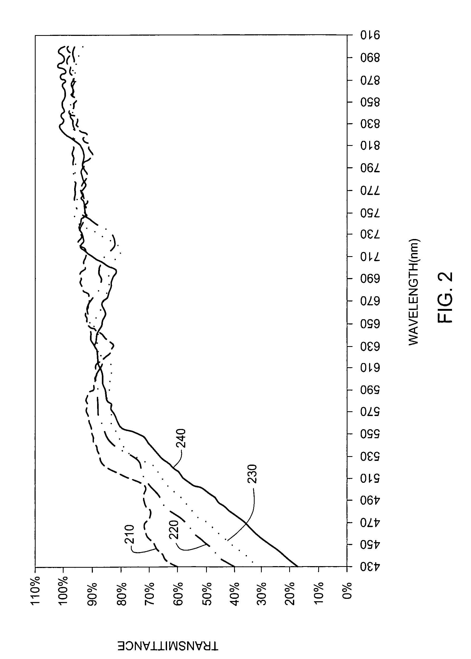
[0101] The invention describes a method of depositing a carbon-containing material layer at a low temperature, such as about 200° C. or lower, onto a large area substrate surface. The invention overcomes the low light transmittance observed at lower wavelengths of between 430 nm and 570 nm as shown in FIG. 2 for a various film thicknesses and provides increased light transmittance of the carbon-containing material layer to about 80% or higher, such as about 90% or higher, about 95% or higher, or about 97% or higher, at all wavelengths in the visible light spectrum. The light transmittance of a carbon-containing material layer without the modification using methods of the invention may become worse when the film gets thicker, as shown in FIG. 2, having a thickness of 0.8 microns, 1.5 microns, 2 microns, and 3.2 microns for line 210, 220, 230, and 240, respectively, where light transmittance were lower as the film get thicker.

[0102]FIG. 7 is a graph for the results of the measured tr...


PUM

PropertyMeasurementUnit
temperatureaaaaaaaaaa
wavelengthsaaaaaaaaaa

Abstract

A method for depositing a carbon-containing material layer onto a substrate includes delivering a mixture of precursors for the carbon-containing material layer into a process chamber, doping the carbon-containing material layer with silicon, and depositing the carbon-containing material layer at low temperature. In one aspect, improved light transmittance of the carbon-containing material layer at all wavelengths of a visible light spectrum is obtained. In addition, a method for depositing an encapsulating layer is provided for various display applications which require low temperature deposition process due to thermal instability of underlying materials used. The encapsulating layer may include one or more barrier layer material layers and one or more amorphous carbon material layers. The amorphous carbon material can be used to reduce thermal stress and prevent the deposited thin film from peeling off the substrate.

Description

CROSS-REFERENCE TO RELATED APPLICATIONS [0001] This application is a continuation-in-part of co-pending U.S. patent application Ser. No. 11 / 133,180, titled “Improving Water Barrier Performance of an Encapsulating Film” (AMAT / 8838.P1), filed May 18, 2005, which is a continuation-in-part of co-pending U.S. patent application Ser. No. 10 / 876,440, titled “Method to improve water-barrier performance by changing film surface morphology” (AMAT / 8838), filed Jun. 25, 2004. The aforementioned related patent applications are herein incorporated by reference.BACKGROUND OF THE INVENTION [0002] 1. Field of the Invention [0003] Embodiments of the present invention generally relate to the deposition of thin films using chemical vapor deposition processing. More particularly, this invention relates to a process for depositing thin films onto large area substrates. [0004] 2. Description of the Related Art [0005] Organic light emitting diode (OLED) displays have gained significant interest recently in...

Claims


Application Information

Patent Timeline
Patent Type & Authority Applications(United States)
IPC IPC(8): C23C16/00H05H1/24
CPCC23C8/36C23C16/26C23C16/345C23C28/00C23C28/046C23C28/42H01L51/5256H10K50/8445C23C16/00H05H1/24
Inventor WON, TAE KYUNGYADAV, SANJAY
Owner APPLIED MATERIALS INC
Why Eureka
Try Eureka