Dry etching apparatus and a method of manufacturing a semiconductor device

a technology of dry etching apparatus and semiconductor device, which is applied in the direction of electrical apparatus, electric discharge tubes, basic electric elements, etc., can solve the problems of unstable discharge, low ion current density and stable discharge, and difficulty in making low ion current density and uniform discharge, etc., to achieve easy concentration of electric field and improve ignitionability

Inactive Publication Date: 2006-05-11
HITACHI LTD
View PDF9 Cites 1 Cited by
  • Summary
  • Abstract
  • Description
  • Claims
  • Application Information

AI Technical Summary

Benefits of technology

[0016] And, it may be controlled, when the plasma discharge is ignited it becomes the concave ECR plane in viewing from the antenna, and after the ignition it becomes the convex ECR plane. Because the ignitionability of the plasma discharge is bad in case of the convex ECR plane, and it is good in case of the concave ECR plane. Especially, the ignitionability is improved, when the intersection point between ECR plane and shower plate exists outside of the antenna diameter. It is possible to control the corrugated surface in such ECR plane by controlling the magnetic coil of the support periphery.
[0017] (4) In addition, when the plasma density becomes the outside high distribution, it is achieved that establishes the cavity division height not less than 30 mm in the antenna back surface. By doing like this, it is possible that it eases the concentration of the electric field in the circumference, and that it solves outside high distribution of the plasma density. Then, the in-plane distribution of the ion current density is equalized and would be able to achieve the in-plane equalizing of the etching rate.

Problems solved by technology

However, in conventional effective magnetic field plasma generator, in condition of the low pressure, it was difficult to make the discharge of low ion current density and stably uniformity.
Therefore, in the condition of the low-pressure low ion current, it was frequently dislocated between the modes in which the plasma existed, and it was proven that the discharge is not stabilized.

Method used


Image

  • Dry etching apparatus and a method of manufacturing a semiconductor device
  • Dry etching apparatus and a method of manufacturing a semiconductor device
  • Dry etching apparatus and a method of manufacturing a semiconductor device

Examples


embodiment 1

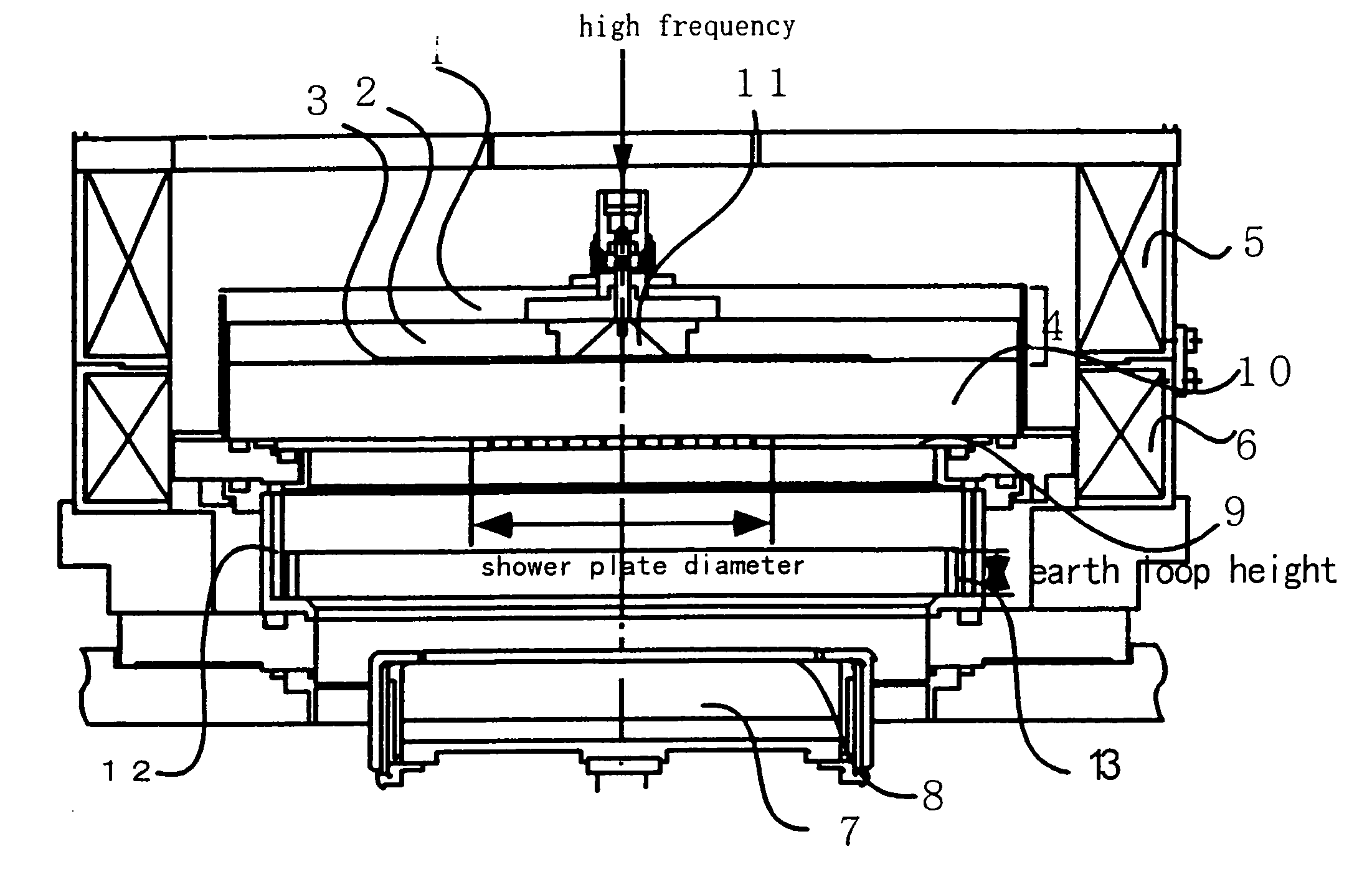
[0042]FIG. 1 is example of dry etching apparatus of this invention.

[0043] In this apparatus, the plasma of the reactive gas is formed in the vacuum chamber by the electron cyclotron resonance between electromagnetic wave which MSA4 radiates and magnetic field which is formed by solenoidal coil 5,6. Samples 8 is processed by irradiating this plasma in samples 8 retained on support 7. The supply of the uniform reactive gas is possible by supplying the reactive gas from shower plates 9 arranged for the plane which faced the sample. And, the generation of the high-density plasma on the edge of discoidal electrodes 3 by the near field is suppressed by installing MSA 4 in atmosphere side of dielectrics 10 which separates the inside in the vacuum chamber from the outside. And, the following can be also prevented: Change of characteristics by the corrosion of discoidal electrodes 3 and pollution of the sample by corrosion reaction product of discoidal electrodes 3. In this embodiment, quar...

embodiment 2

[0047] This embodiment describes formation method of ECR magnetic field where plasma density of the circumference increases, as it is above mentioned.

[0048]FIG. 7 shows the direction of the electric field in case of antenna structure of embodiment 1. In this structure, about the electric field, the length direction in the central part and the lateral in the periphery are generated. Therefore, like FIG. 8, when there is a magnetic field in length direction of the size which generates electron cyclotron resonance, since resistant resonance are generated in the circumference which orthogonalizes electric field and magnetic field, it is possible that the plasma density of the circumference increases. In order to make such magnetic field, like solenoidal coils 6 of FIG. 8, the solenoidal coil whose upper end plane is higher than discoidal conductors 3, whose lower end plane is lower than the shower plate lower end, which cover the circumference of shower plate from the antenna is needed...

embodiment 3

[0050] In this embodiment, the method to decrease central plasma density as mentioned above.

[0051] When divergence magnetic field like FIG. 10 was used, since it diffuses in the circumference direction as the plasma accords with magnetic field, the central plasma density can be reduced. It could be realized by installing solenoidal coil 14 whose inside diameter is small at MSA 4 upper part, in order to make such divergence magnetic field.

[0052] The relationship between inside diameter of solenoidal coil 14 and uniformity is shown in FIG. 11. Wafer in-plane distribution of the ion current density takes the positive value which shows the crown, when the inside diameter of solenoidal coil is bigger than the antenna diameter, even if the coil current is increased. From the point that inside diameter is less than 255 mm of antenna diameter, the uniformity would change, as it is dependent on the coil current. As the current is increased, it would be able to adjust from the positive unif...


PUM

PropertyMeasurementUnit
distanceaaaaaaaaaa
diameteraaaaaaaaaa
pressureaaaaaaaaaa

Abstract

The processing with a low gate rate of destruction and high anisotropy is achieved in dry etching. Plasma is generated by ECR resonance of electromagnetic wave which arose by supplying Ultra High Frequency electric power in microstripline 4 arranged on the atmosphere side of a dielectric 2, which separates a vacuum inside and an outside and magnetic field. A conducting layer is etched by this plasma, which is stable and uniform plasma.

Description

BACKGROUND OF THE INVENTION [0001] 1. Field of the Invention [0002] This invention concerns the production technique of a semiconductor device, including dry etching processes of the wiring of the semiconductor device using effective magnetic field plasma generator for the dry etching process and this magnetic field plasma generator. [0003] 2. Description of the Related Art [0004] Until now, an effective magnetic field plasma generator has been used for the process of the plasma treatment used in the manufacturing of a semiconductor device. For example, this effective magnetic field plasma generator has been described in Laid Open No. 8-337887 and Laid Open No. 9-321031. [0005] Laid Open No. 8-337887 disclosed, as shown in FIG. 2, the microstrip antenna (MSA) comprising a discoidal electrode 1 which was grounded, dielectric 2, and a high frequency discoidal electrodes 3 installed to face discoidal electrode 1 through a dielectric. The plasma of the reactive gas was formed by electro...

Claims


Application Information

Patent Timeline
Patent Type & Authority Applications(United States)
IPC IPC(8): H01L21/306C23F1/00H01L21/302C23F4/00H01J37/32H01L21/00H01L21/3065H01L21/3213
CPCH01J37/32082H01L21/32136H01L21/32137H01L21/67069H01L21/3065
Inventor KOFUJI, NAOYUKIMORI, MASAHITOYOKOGAWA, KEN'ETSUITABASHI, NAOSHITSUJIMOTO, KAZUNORITACHI, SHIN'ICHI
Owner HITACHI LTD
Why Eureka
Try Eureka